UART0 to UART2
M30240 Group
Rev.1.00 Sep 24, 2003 Page 87 of 360
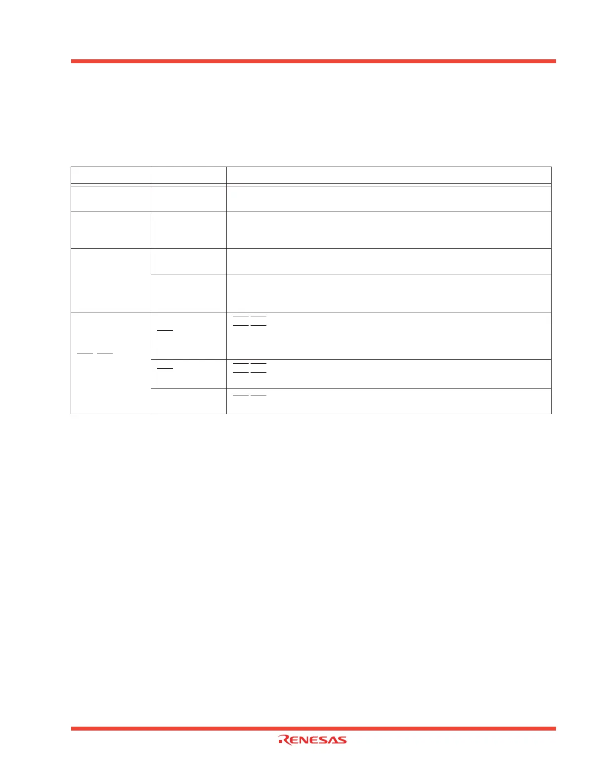
Table 1.26 lists the functions of the input/output pins during clock synchronous serial I/O mode. This
table shows the pin functions when the transfer clock output from multiple pins function is not selected.
Note that for a period from when the UARTi operation mode is selected to when transfer starts, the
TxD pin outputs a “H”. The typical clock synchronous timing diagrams are shown in Figure 1.82.
Table 1.26: IART mode input/output pin functions
Pin name Function Method of selection
TxDi
(P6
3
, P6
7
, P7
0
)
Serial data
output
(Outputs dummy data when performing reception only)
RxDi
(P6
2
, P6
6
, P7
1
)
Serial data input
Port P6
2
, P6
6
, and P7
1
direction register (bits 2 and 6 at address 03EE
16
bit 1 at address
03EF
16
)= “0”
(Can be used as an input port when performing transmission only.)
CLKi
(P6
1
, P6
5
, P7
2
)
Transfer clock
output
Internal/external clock select bit (bit 3 at address 03A0
16
, 03A8
16
, 0378
16
) = “0”
Transfer clock
input
Internal/external clock select bit (bit 3 at address 03A0
16
, 03A8
16
, 0378
16
) = “1”
Port P6
1
, P6
5
, and P7
2
direction register (bits 1 and 5 at address 03EE
16
, bit 2 at address
03EF
16
) = “0”
CTS
i/RTSi
(P6
0
,P6
4
,P7
3
)
CTS
input
CTS
/RTS disable bit (bit 4 at address 03A4
16
, 03AC
16
, 037C
16
) = “0”
CTS
/RTS function select bit (bit 2 at address 03A4
16
, 03AC
16
, 037C
16
) = “0”
Port P6
0
, P6
4
and P7
3
direction register (bits 0 and 4 at address 03EE
16
, bit 3 at address
03EF
16
) = “0”
RTS
output
CTS
/RTS disable bit (bit 4 at address 03A4
16
, 03AC
16
, 037C
16
) = “0”
CTS
/RTS function select bit (bit 2 at address 03A4
16
, 03AC
16
, 037C
16
) = “1”
Programmable I/
O port
CTS
/RTS disable bit (bit 4 at address 03A4
16
, 03AC
16
, 037C
16
) = “1”
 Loading...


