UART0 to UART2
M30240 Group
Rev.1.00 Sep 24, 2003 Page 93 of 360
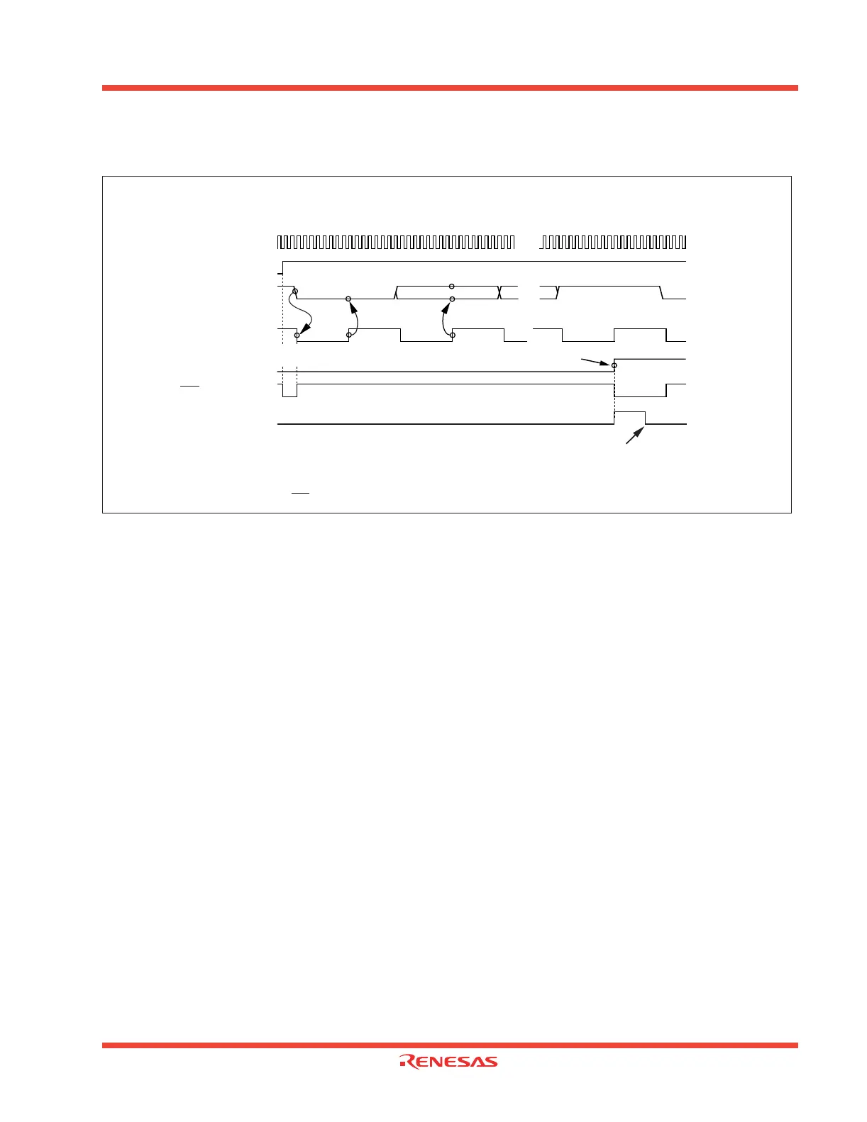
Figure 1.88 and Figure 1.89 show the typical UART mode transmit and receive timing diagrams.
Figure 1.88: Typical receive timing in UART mode
D0
Start bit
Sampled “L”
Receive data taken in
BRGi count
source
Receive enable bit
RxDi
Transfer clock
Receive
complete flag
RTSi
Stop bit
“1”
“0”
“0”
“1”
“H”
“L”
The above timing applies to the following settings :
•Parity is disabled.
•One stop bit.
•RTS function is selected.
Receive interrupt
request bit
“0”
“1”
Transferred from UARTi receive register to
UARTi receive buffer register
Reception triggered when transfer clock
is generated by falling edge of start bit
D7D1
Cleared to “0” when interrupt request is accepted, or cleared by software
Example of receive timing when tranfer data is 8 bits long (parity disabled, one-stop bit)
.......
.......
.......
 Loading...


