UART0 to UART2
M30240 Group
Rev.1.00 Sep 24, 2003 Page 95 of 360
1.2.23.2.1 Sleep mode (UART0, UART1)
This mode is used to transfer data between specific microcomputers among multiple microcomputers con-
nected using UARTi. The sleep mode is selected when the sleep select bit (bit 7 at addresses 03A0
16
, 03A8
16
)
is set to “1” during reception. In this mode, the unit performs receive operation when the MSB of the received
data = “1” and does not perform receive operation when the MSB = “0”.
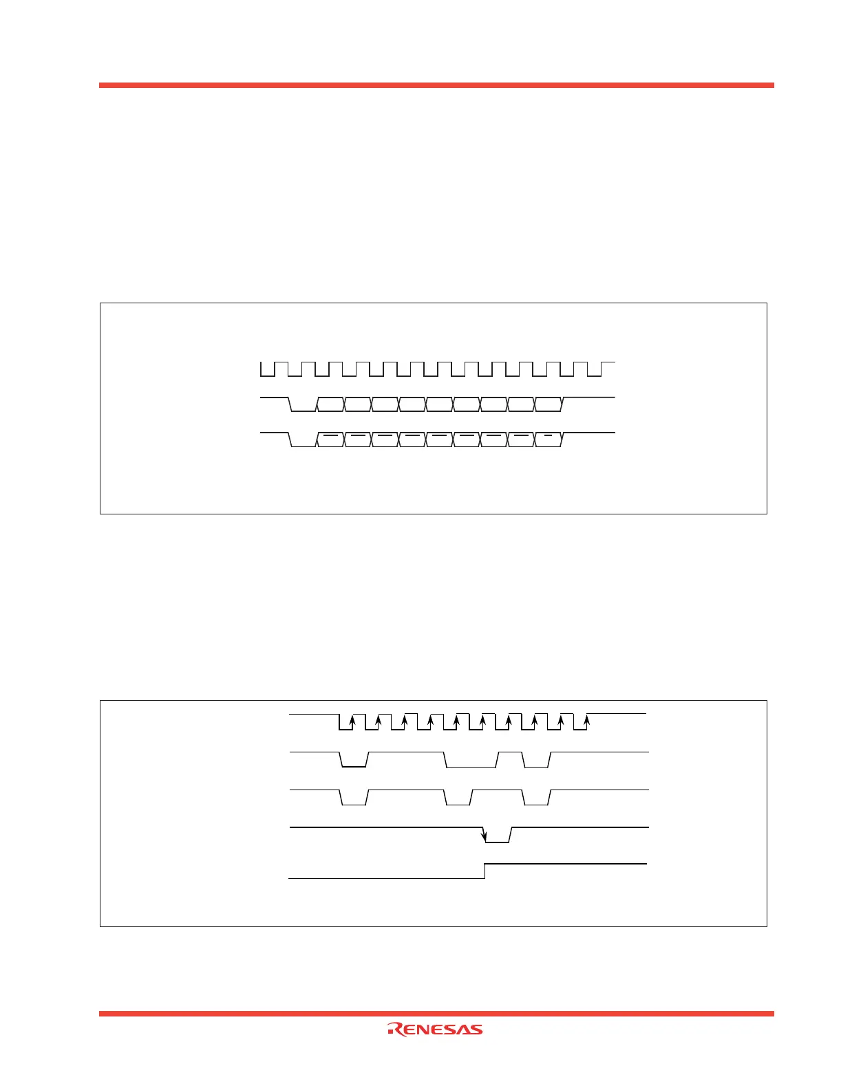
1.2.23.2.2 Function for switching serial data logic (UART2)
When the data logic select bit (bit 6 of address 037D
16
) is assigned 1, data is inverted in writing to the trans-
mission buffer register or reading the reception buffer register. Figure 1.90 shows the example of timing for
switching serial data logic.
Figure 1.90: Timing for switching serial data logic
1.2.23.2.3 TxD, RxD I/O polarity reverse function (UART2)
This function is to reverse TxD pin output and RxD pin input. The level of any data to be input or output (in-
cluding the start bit, stop bit(s), and parity bit) is reversed. Set this function to “0” (not to reverse) for usual use.
1.2.23.2.4 Bus collision detection function (UART2)
This function is to sample the output level of the TxD pin and the input level of the RxD pin at the rising edge
of the transfer clock; if their values are different, then an interrupt request occurs. Figure 1.91 shows the ex-
ample of detection timing of a buss collision (in UART mode).
Figure 1.91: Detection timing of a bus collision (in UART mode)
ST : Start bit
P : Even parity
SP : Stop bit
D0
D1 D2 D3 D4 D5 D6 D7 P SPST
SPST D3 D4 D5 D6 D7 PD0 D1 D2
Transfer clock
TxD
2
(no reverse)
TxD2
(reverse)
“H”
“L”
“H”
“L”
“H”
“L”
Example of timing for switching serial data logic when LSB is first (parity enabled, one-stop bit)
ST : Start bit
SP : Stop bit
ST
ST
SP
SP
Transfer clock
TxD
2
RxD2
Bus collision detection
interrupt request signal
“H”
“L”
“H”
“L”
“H”
“L”
“1”
“0”
Bus collision detection
interrupt request bit
“1”
“0”
 Loading...


