57
2017/06
10.5 Register Mapping of the TBEN-L Devices
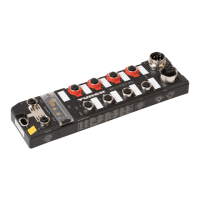
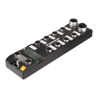
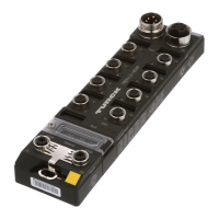
10.5.1 TBEN-Lx-16DIP/TBEN-L4-16DIN
Meaning of the Register Bits, page 61.
Register Byte Bit 7 Bit 6 Bit 5 Bit 4 Bit 3 Bit 2 Bit 1 Bit 0
Packed input data
0x0000
Inputs
Byte 0 DI7
C3P2
DI6
C3P4
DI5
C2P2
DI4
C2P4
DI3
C1P2
DI2
C1P4
DI1
C0P2
DI0
C0P4
Byte 1 DI15
C7P2
DI14
C7P4
DI13
C6P2
DI12
C6P4
DI11
C5P2
DI10
C5P4
DI9
C4P2
DI8
C4P4
0x0001
Status word
Byte 0
–------
Diag
Warn
Byte 1 – FCE – - CFG COM V
1
–
0x0002
group diag-
nostics
Byte 0–------I/O Diag
Byte 1
–-------
Inputs
0x8000 Byte 0 DI7
C3P2
DI6
C3P4
DI5
C2P2
DI4
C2P4
DI3
C1P2
DI2
C1P4
DI1
C0P2
DI0
C0P4
Byte 1 DI15
C7P2
DI14
C7P4
DI13
C6P2
DI12
C6P4
DI11
C5P2
DI10
C5P4
DI9
C4P2
DI8
C4P4
Diagnostics
0xA000 Byte 0 SCS7 SCS6 SCS5 SCS4 SCS3 SCS2 SCS1 SCS0
Byte 1–-------
Parameters
0xB000Byte 0–-------
Byte 1–-------
0xB001 Byte 0 Inv. DI7 Inv. DI6 Inv. DI5 Inv. DI4 Inv. DI3 Inv. DI2 Inv. DI1 Inv. DI0
Byte 1 Inv. DI15 Inv. DI14 Inv. DI13 Inv. DI12 Inv. DI11 Inv. DI10 Inv. DI9 Inv. DI8
0xB002 Byte 0 reserved
Byte 1 Pulse stretching input 0
0xB003 Byte 0 Pulse stretching input 1
Byte 1 Pulse stretching input 2
0xB004 Byte 0 Pulse stretching input 3
Byte 1 Pulse stretching input 4
0xB009 Byte 0 Pulse stretching input 13
Byte 1 Pulse stretching input 14
0xB00A Byte 0 Pulse stretching input 15
Byte 1 reserved
 Loading...