14.BCD DATA OUTPUT(OPTION)
93
14-2. Logic Change
Select the logic of output signals with pin No. 28.
When COM and pin No. 28 are open: negative logic
When they are short-circuited: positive logic
14-3. BCD Data Hold
The BCD data output signal is held. Switching is carried out by pin No. 27.
When COM and pin No. 27 are open: hold cancel
When they are short-circuited: hold on
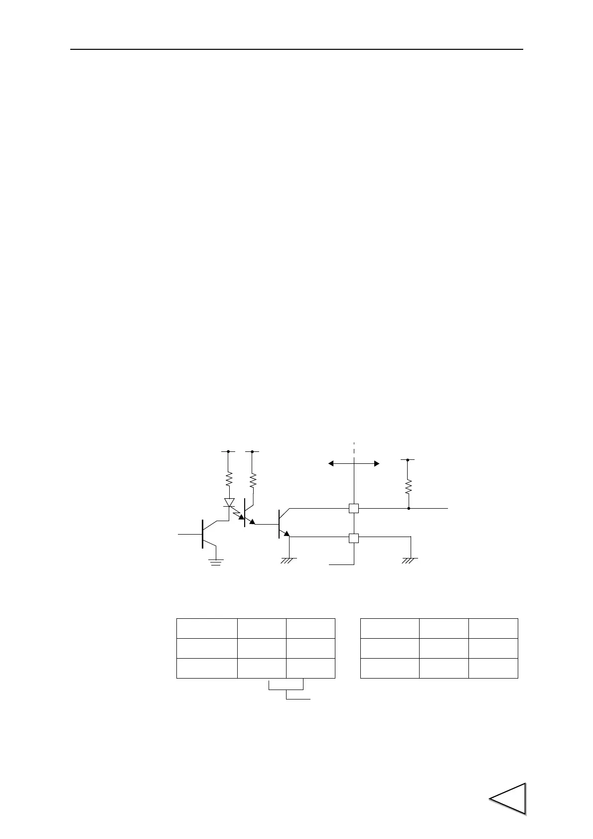
14-4. Equivalent Circuit
・Output
The signal output circuit is operated through a TTL open collector.
F371
Inside
Vcc
+5V
COM
Ve xt
Vceo=30V(max)
Ic =30mA (max)
● Internal transistor status
Output data Negative Positive
0OFFON
1ONOFF
● Output pin level
Output data Negative Positive
0
HL
1
LH
Through logic switching(pin28)
Outside

 Loading...