228 www.xilinx.com Virtex-5 RocketIO GTP Transceiver User Guide
UG196 (v1.3) May 25, 2007
Chapter 11: Design Constraints Overview
R
To calculate the blocking capacitor value, several factors must be known:
• t
r
: The rise time of the signal
• T: The bit period
• N
CID
: The maximum number of consecutive identical digits (CIDs)
• PDJ: The amount of pattern dependent jitter that can be tolerated by the system
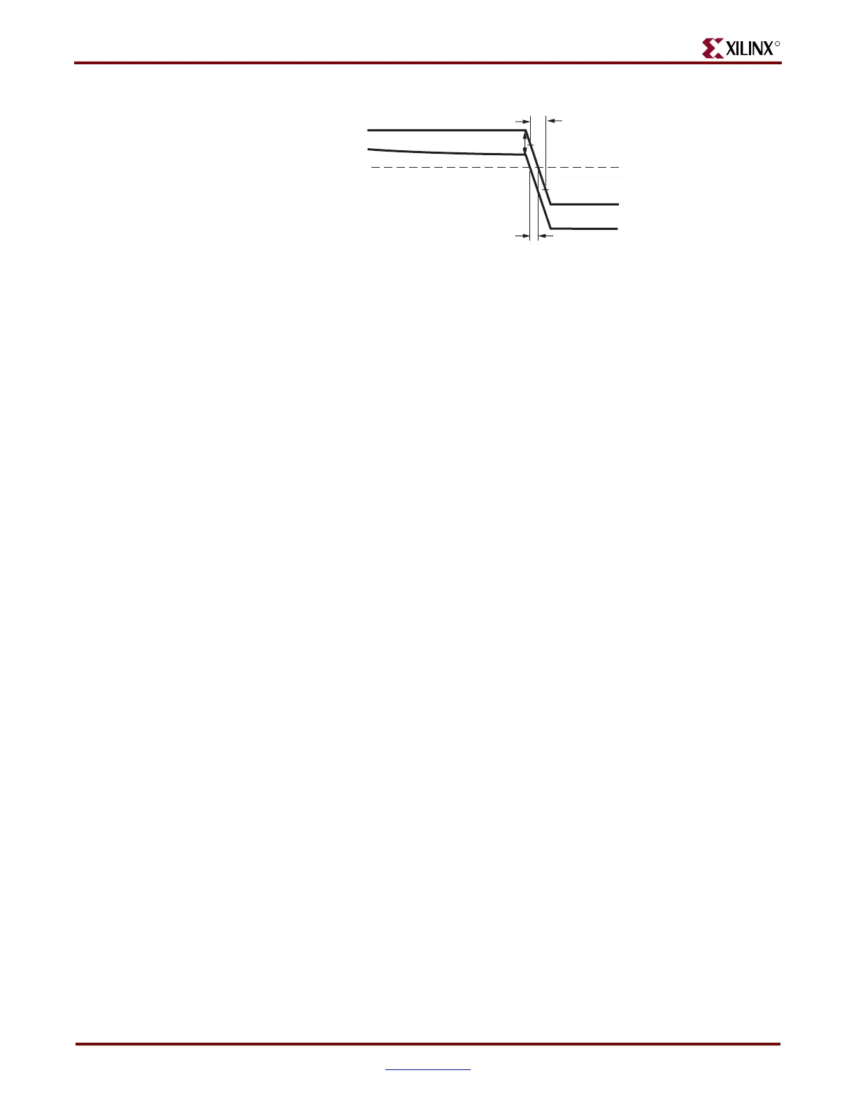
From Figure 11-5 it can be seen that PDJ can be estimated by:
Equation 11-1
The voltage drop can be calculated using Equation 11-2:
Equation 11-2
where:
•τ is the RC time constant (C is the ac coupling capacitor, R = 2 x R
TERM
).
• t is the total discharge time, which is equal to N
CID
T.
The slope is defined by Equation 11-3:
Equation 11-3
Substituting Equation 11-2 and Equation 11-3 into Equation 11-1 and solving for C gives:
Equation 11-4
To demonstrate the use of Equation 11-4, calculate the blocking capacitor value needed for
a serial link running at 3.125 Gb/s using 8B/10B line coding. This example uses the
following assumptions:
• Bit period (T) = 3.200 x 10
-10
(3.125 Gb/s)
• Signal rise time (t
r
) = 6.400 x 10⁻¹¹ (0.2 UI)
• Pattern Dependent Jitter (PDJ) = 3.200 x 10⁻¹² (0.01 UI)
• Consecutive Identical Digits (N
CID
) = 5 (guaranteed by 8B/10B)
• Termination Resistance (R
TERM
) = 75 Ω
Figure 11-5: PDJ Detail
VTH
UG196_c11_05_092006
V2
V1
ΔV
PDJ
20%
80%
t
r
PDJ
VΔ
slope
-------------=
VΔ 0.5V
PP
1 e
t– τ⁄
–()=
slope V
PP
0.6
t
r
-------
×=
C
T– N
CID
×
2 R
TERM
× 1
1.2PDJ
t
r
------------------–
⎝⎠
⎛⎞
ln×
--------------------------------------------------------------------------=
 Loading...

