234 www.xilinx.com Virtex-5 RocketIO GTP Transceiver User Guide
UG196 (v1.3) May 25, 2007
Chapter 12: PCB Materials and Traces
R
The same W/S ratio also must be less than 0.8, otherwise strong coupling between the
traces requires narrower, lossier traces for a Z
0O
of 50Ω. To clarify, with Z
0O
at 50Ω, an
even mode impedance (Z
0E
) of 60Ω or below is desired.
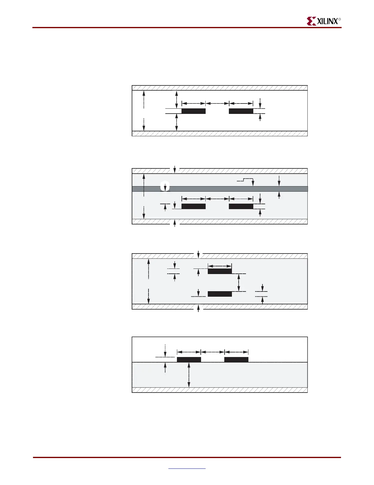
Figure 12-1 through Figure 12-4 show example cross sections of differential structures.
A good PCB manufacturer understands controlled impedance and allows fine adjustments
for line widths to produce a Z
0O
of 50Ω. The PCB manufacturer also provides the
parameters necessary for the specific PCB layout. Some parameters can be calculated or
Figure 12-1: Differential Edge-Coupled Centered Stripline
Figure 12-2: Differential Edge-Coupled Offset Stripline
Figure 12-3: Centered Broadside-Coupled Stripline
Figure 12-4: Differential Microstrip
UG196_c12_01_051406
h
h
wws
Er
t
d=2h+t
h
h
wws
Er
t
t
d=3h+2t
h
orthogonal lines
UG196_c12_02_051406
t
t
Er
h
h
w
2h
d=4h+2t
UG196_c12_03_051406
wws
t
Er
Er = 1
h
UG196_c12_04_051406
 Loading...

