260 www.xilinx.com Virtex-5 RocketIO GTP Transceiver User Guide
UG196 (v1.3) May 25, 2007
Appendix A: MGT to GTP Transceiver Design Migration
R
Reference clock multiplication has also evolved over the transceiver generations from a
limited selection of multiplier values to a fully programmable solution starting with
Virtex-4 devices. Table A-5 shows the clock multiplier values supported in the Virtex-II Pro
devices.
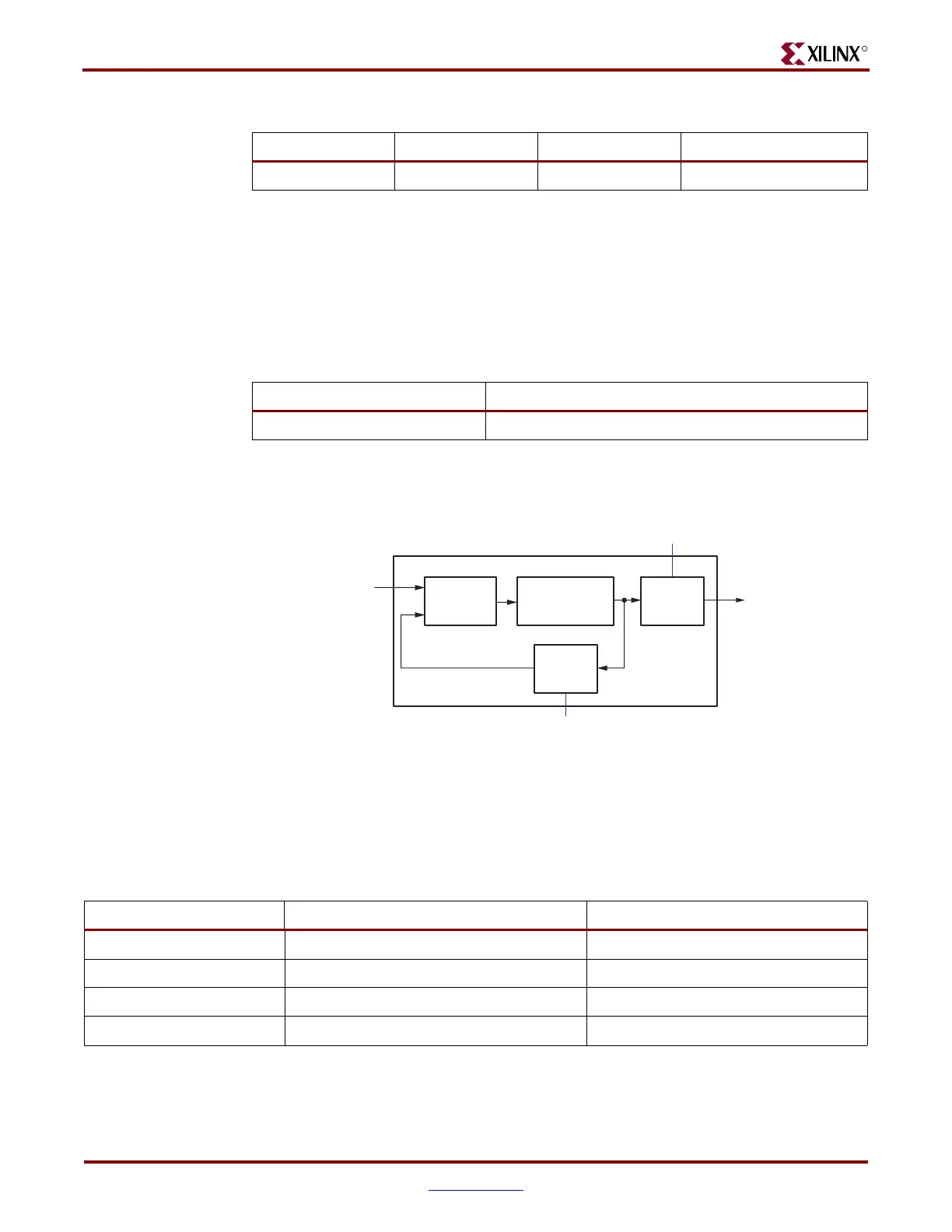
The Virtex-4 and Virtex-5 devices use the circuitry shown in Figure A-2 to multiply the
reference clock.
Table A-6 shows the parameters used to configure the operation of the clock multiplication
circuitry as well as the supported divide values. While Virtex-4 devices support separate
multiply ratios for transmit and receive operations, one multiply ratio is used for both in
Virtex-5 devices.
Others Yes
(2)
Yes
(2)
Yes
(2)
Notes:
1. Encoding and clocks must be done in the FPGA logic.
2. Depending on encode, some functionality must be done in the FPGA logic.
Tab le A - 5 : Virtex-II Pro Clock Multipliers
Supported Clock Multiplier Values
Virtex-II Pro FPGA 20
Figure A-2: Virtex-4 and Virtex-5 Clock Multiplication Circuitry
Tab le A - 4 : Encoding Support (Continued)
Encoding Schemes Virtex-II Pro MGT Virtex-4 MGT Virtex-5 GTP Transceiver
Phase
Frequency
Detector
Charge Pump,
Loop Filter,
VCO
Ref Clk
PLL
Divide By M
Parameter
Divide by
N
Divide by
M
Divide By N
Parameter
Clk Out
UG196_a_02_080606
Table A-6: Virtex-4 and Virtex-5 Clock Multiplication Parameters
Virtex-4 MGT Virtex-5 GTP Transceiver
Divide by M Parameter TXPLLNDIVSEL, RXPLLNDIVSEL PLL_DIVSEL_FB
Divide by M Values 8, 10, 16, 20, 32, 40 1, 2, 3, 4, 5
Divide by N Parameter TXOUTDIV2SEL, RXOUTDIV2SEL PLL_DIVSEL_REF
Divide by N Values 1, 2, 4, 8, 16, 32 1, 2
 Loading...

