314 www.xilinx.com Virtex-5 RocketIO GTP Transceiver User Guide
UG196 (v1.3) May 25, 2007
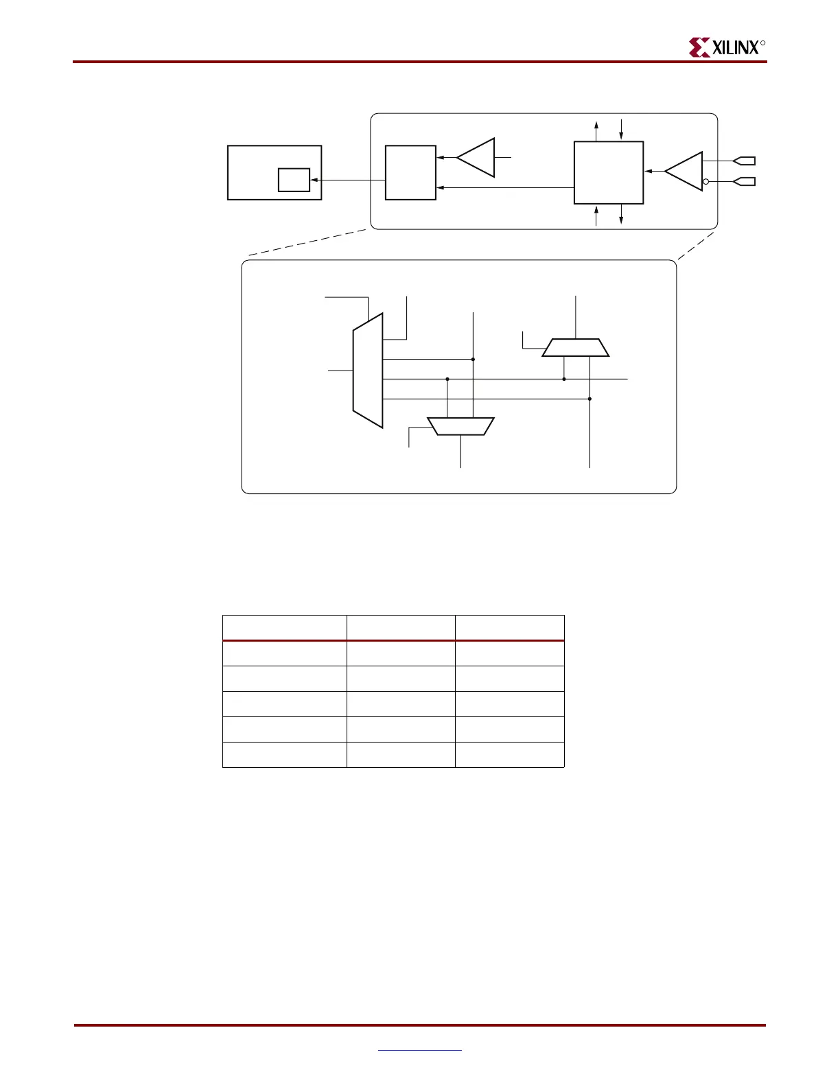
Appendix F: Advanced Clocking
R
All the MUX selectors reside in address 0x04 of the DRP and are mapped as shown in
Table F-1.
To ensure that other attributes in DRP address 0x04 are not accidentally changed, use a
read/modify/write procedure to change the MUX selectors.
Figure F-1: Reference Clock Multiplexing Stucture
Table F-1: MUX Selector
REFCLK_SEL Bit Address
REFCLK_SEL[0] 6
0x04
REFCLK_SEL[1] 5 0x04
REFCLK_SEL[2] 4 0x04
CLKSOUTH_SEL 7 0x04
CLKNORTH_SEL 8 0x04
GTP_DUAL Tile
Clock
Muxing
XX0
10
10
001
011
1X1
BUFG/BUFR
IBUFDS
CLKP
CLKIN
CLKIN
CLKP
CLKN
REFCLK_SEL
Global Clock
(GREFCLK)
CLKINSOUTH
CLKOUTNORTH
CLKINNORTHCLKOUTSOUTH
CLKSOUTH_SEL
CLKNORTH_SEL
GREFCLK
A PLL
GTP
Dedicated
Clock
Routing
CLKN
UG196_af_01_032307
 Loading...

