171
ABOV Semiconductor Co., Ltd.
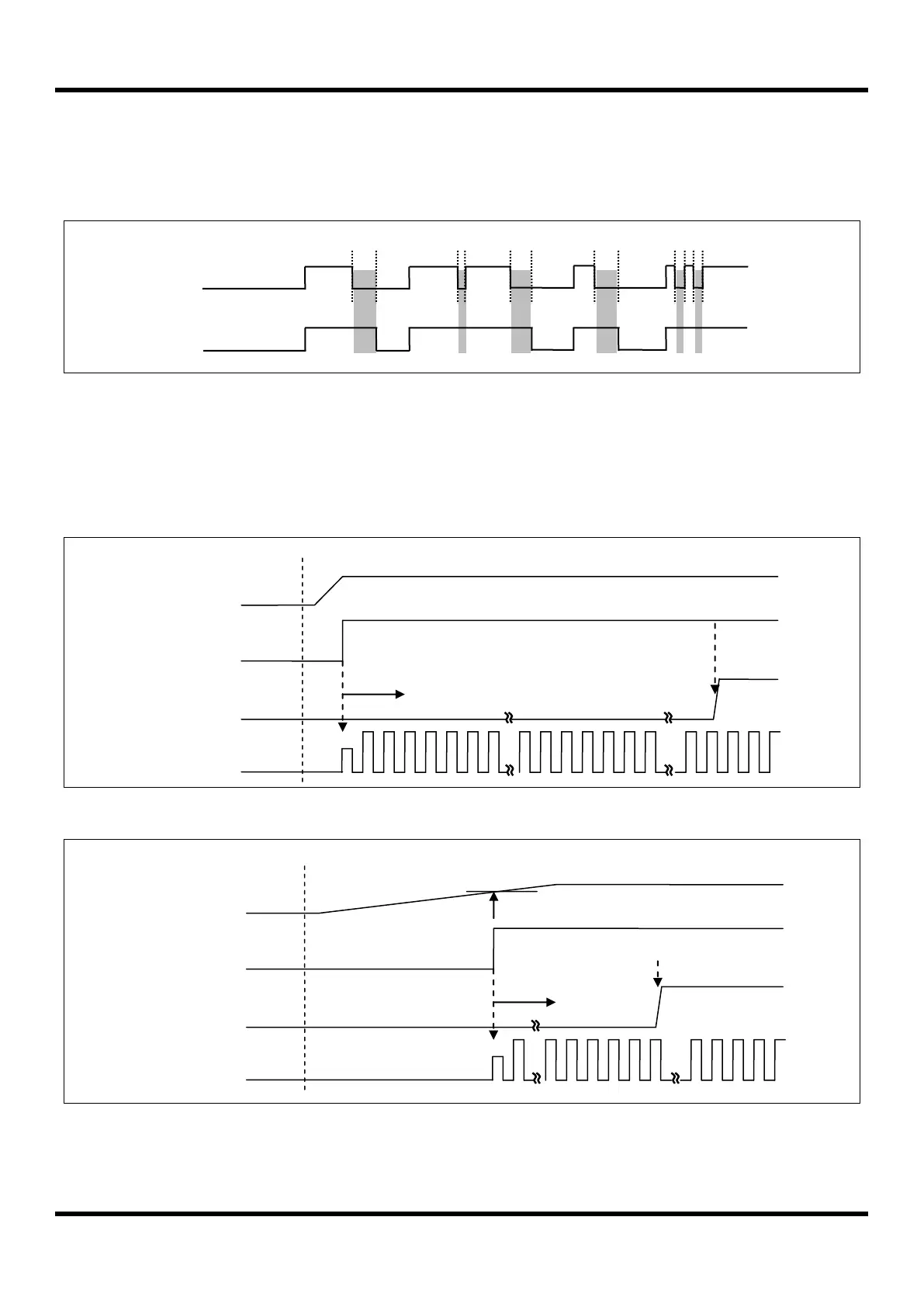
13.4 RESET Noise Canceller
The Figure 13.2 is the noise canceller diagram for noise cancellation of RESET. It has the noise cancellation value of
about 2us(@V
DD
=5V) to the low input of system reset.
Figure 13.2 Reset noise canceller timer diagram
13.5 Power on RESET
When rising device power, the POR (Power On Reset) has a function to reset the device. If POR is used, it executes
the device RESET function instead of the RESET IC or the RESET circuits.
Figure 13.3 Fast VDD Rising Time
Figure 13.4 Internal RESET Release Timing On Power-Up
Slow VDD Rise Time, min. 0.05V/ms
Fast VDD Rise Time, max. 30.0V/ms

 Loading...


