11
ABOV Semiconductor Co., Ltd.
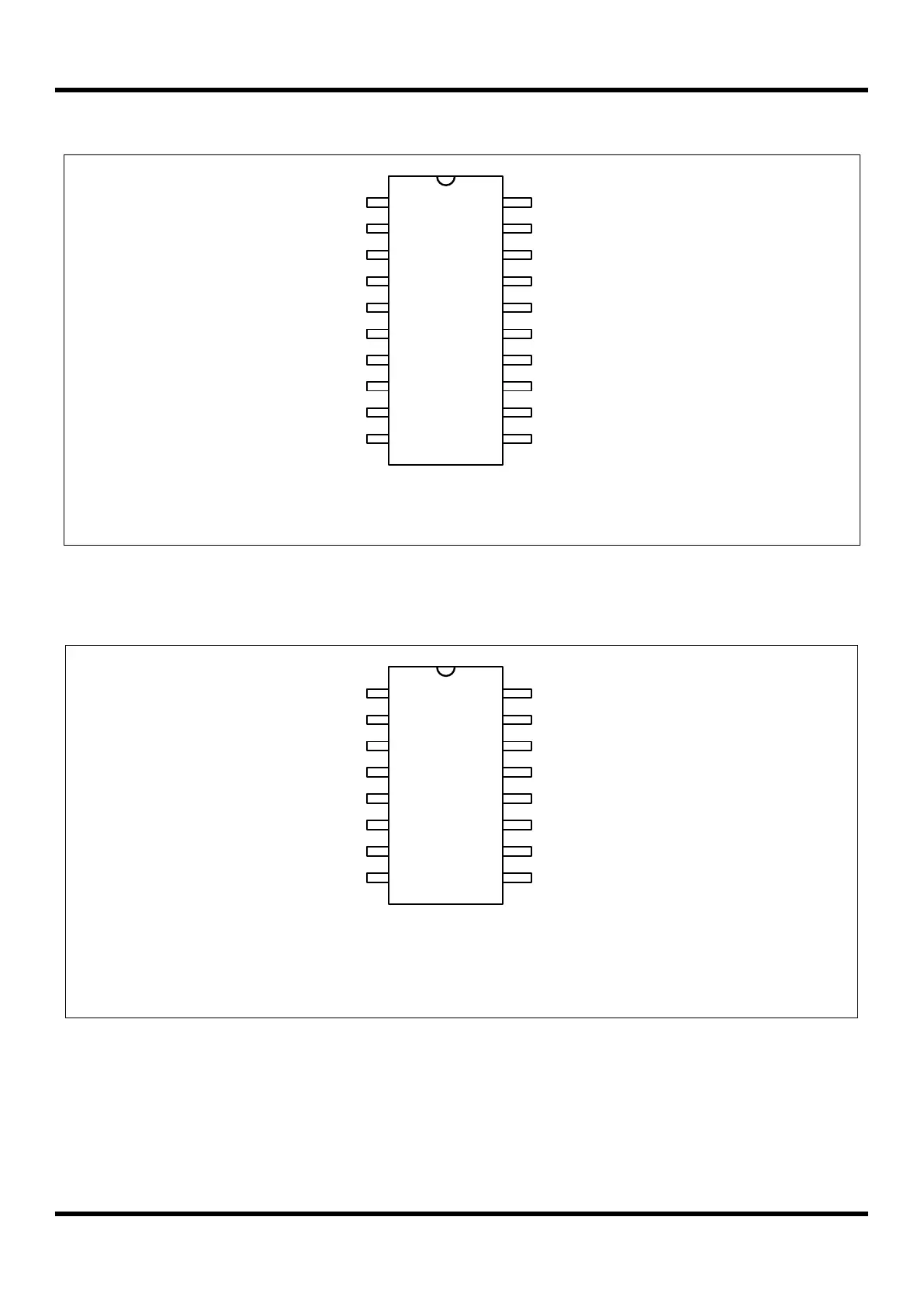
3 Pin assignment
MC96F8204D/R
(20-SOP/TSSOP)
1
2
3
4
18
17
20
19
VDD
P06/AN6/SS/XIN/SXIN
P05/AN5/AVREF/EC1/RESETB
VSS
P07/AN7/SCK/XOUT/SXOUT
P01/AN1/EINT1/RXD/MISO/DSCL
P00/AN0/EINT0/TXD/MOSI/DSDA
P02/AN2/EINT11/T1O/PWM1O
5
16
P04/AN4/EINT10/EC2/SDA P03/AN3/EINT12/T2O/PWM2O/SCL
6
P21
7
P20
15
P10/(SDA)
14
P11/(SCL)
8
9
10
13
12
11
P12/(TXD/MOSI)
P13/(RXD/MISO)
P14/(SCK)
P17
P16
P15
NOTE)
1. On On-Chip Debugging, ISP uses P0[1:0] pin as DSCL, DSDA.
Figure 3.1 MC96F8204D 20SOP/TSSOP Pin Assignment
MC96F8204M
(16-SOPN)
1
2
3
4
14
13
16
15
VDD
P06/AN6/SS/XIN/SXIN
P05/AN5/AVREF/EC1/RESETB
VSS
P07/AN7/SCK/XOUT/SXOUT
P01/AN1/EINT1/RXD/MISO/DSCL
P00/AN0/EINT0/TXD/MOSI/DSDA
P02/AN2/EINT11/T1O/PWM1O
5
12
P04/AN4/EINT10/EC2/SDA P03/AN3/EINT12/T2O/PWM2O/SCL
6
P15
7
P14/(SCK)
11
P10/(SDA)
10
P11/(SCL)
8 9
P12/(TXD/MOSI)P13/(RXD/MISO)
NOTE)
1. On On-Chip Debugging, ISP uses P0[1:0] pin as DSCL, DSDA.
2. The P16-P17 and P20-P21 pins should be selected as a push-pull output or an input with pull-up resistor by
software control when the 16-pin package is used.
Figure 3.2 MC96F8204M 16SOPN Pin Assignment
 Loading...


