23
ABOV Semiconductor Co., Ltd.
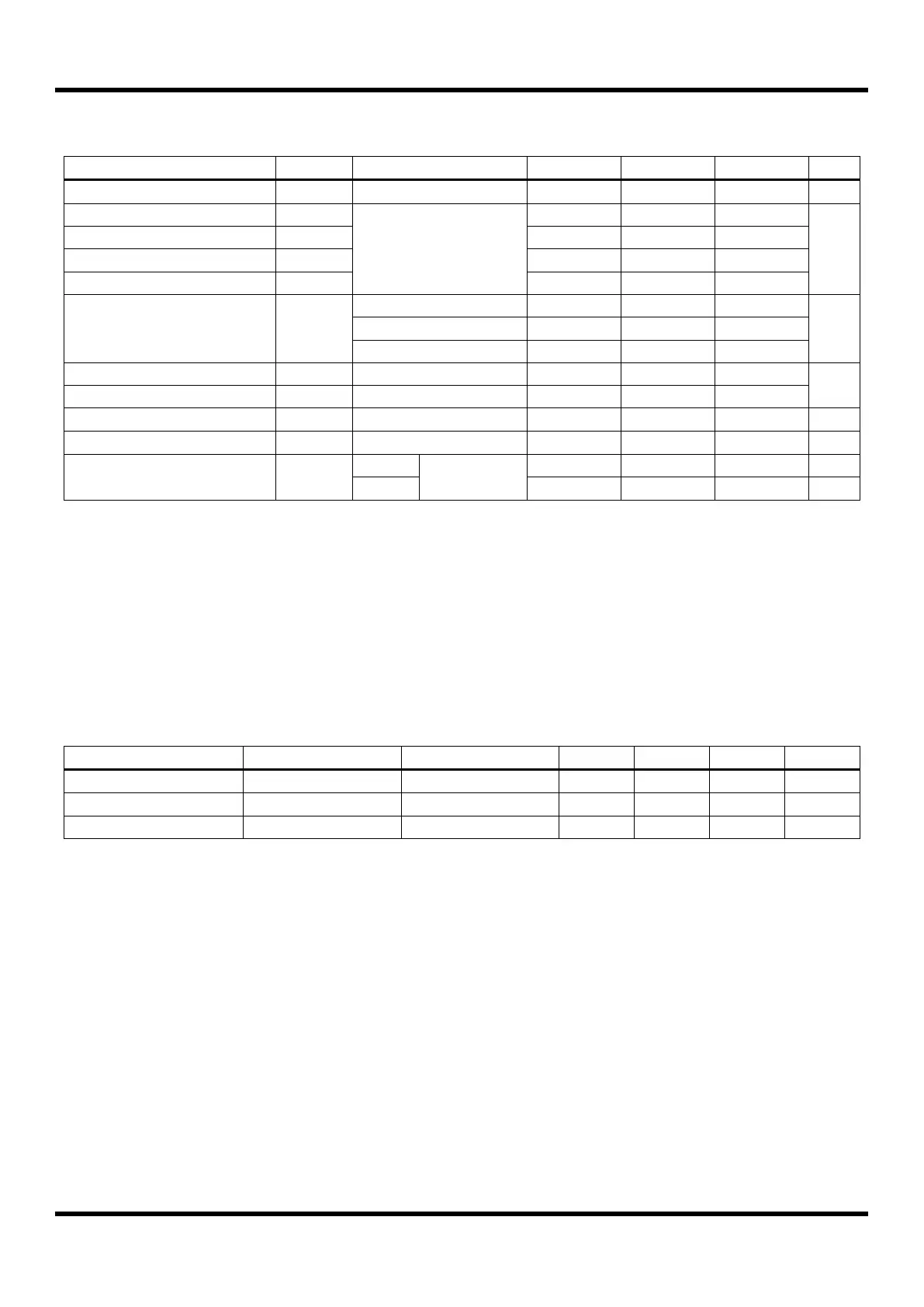
7.3 A/D Converter Characteristics
(T
A
=-40°C ~ +85°C, VDD=1.8V ~ 5.5V, VSS=0V)
AVREF= 2.7V – 5.5V
fx= 8MHz
Differential Linearity Error
A/DC Input Leakage Current
Table 7.3 A/D Converter Characteristics
NOTE)
1. Zero offset error is the difference between 000000000000 and the converted output for zero input
voltage (VSS).
2. Top offset error is the difference between 111111111111 and the converted output for top input voltage
(AVREF).
3. If AVREF is less than 2.7V, the resolution degrades by 1-bit whenever AVREF drops 0.1V.
(@ADCLK = 0.5MHz, Under 2.7V resolution has no test.)
7.4 Power-On Reset Characteristics
(T
A
=-40°C ~ +85°C, VDD=1.8V ~ 5.5V, VSS=0V)
Table 7.4 Power-on Reset Characteristics

 Loading...


