109
ABOV Semiconductor Co., Ltd.
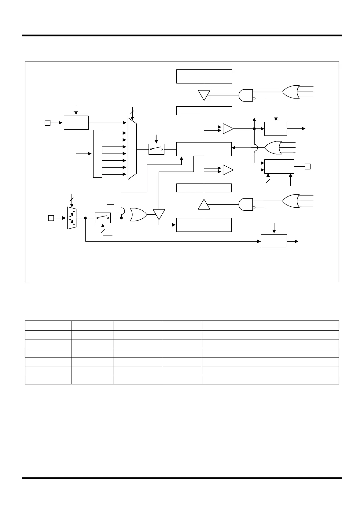
11.6.5 Block Diagram
TnMS[1:0]
TnPOL
Reload
A Match
TnCC
TnEN
Comparator
16-bit Counter
TnCNTH/TnCNTL
16-bit B Data Register
TnBDRH/TnBDRL
Clear
B Match
Buffer Register B
Comparator
16-bit A Data Register
TnADRH/TnADRL
TnIFR
INT_ACK
Clear
A Match
Buffer Register A
Reload
Pulse
Generator
TnO/
PWMnO
R
EINT1n
TnCNTR
TnEN
Clear
POL1n of EIPOL1
FLAG1n
(EIFLAG.m)
INT_ACK
Clear
To interrupt
block
2
2
TnMS[1:0]
2
P
r
e
s
c
a
l
e
r
fx
M
U
X
fx/4
fx/8
fx/512
fx/2048
fx/64
fx/2
Edge
Detector
TnECE
ECn
fx/1
To other block
TnCK[2:0]
3
To interrupt
block
A Match
TnCC
TnEN
RLDnEN
A Match
TnCC
TnEN
RLDnEN
NOTE)
1. The TnEN is automatically cleared to logic “0” after one pulse is generated at a PPG one-shot
mode.
Figure 11.19 16-bit Timer 1/2 Block Diagram(Where n = 1 and 2, m = 3 and 4)
11.6.6 Register Map
Timer n Control High Register
Timer n Control Low Register
Timer n A Data High Register
Timer n A Data Low Register
Timer n B Data High Register
Timer n B Data Low Register
Table 11.8 Timer 1/2 Register Map(Where n = 1 and 2)

 Loading...


