BL702/704/706 Reference Manual
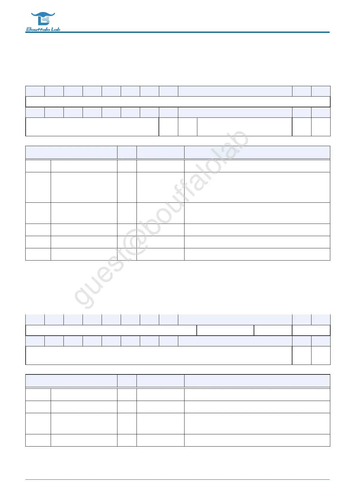
5.4.4 gpdac_ctrl
Address:0x40000308
31 30 29 28 27 26 25 24 23 22 21 20 19 18 17 16
RSVD
15 14 13 12 11 10 9 8 7 6 5 4 3 2 1 0
RSVD REF
SEL
TSEN RSVD BRS
ANA
ARS
ANA
Bits
Name Type Reset Description
31:9 RSVD
8 REFSEL R/W 1’h0 Reference select
1’h0 Internal reference
1’h1 External reference
7 TSEN R/W 1’h0 Test enable 1’h0 analog test disabled (ATEST is set in Hi-Z
state) 1’h1 analog test point enabled to ATEST
6:2 RSVD
1 BRSANA R/W 1’h1 Soft reset for DAC channel B, active low
0 ARSANA R/W 1’h1 Soft reset for DAC channel A, active low
5.4.5 gpdac_actrl
Address:0x4000030c
31 30 29 28 27 26 25 24 23 22 21 20 19 18 17 16
RSVD AOMUX ARNG RSVD
15 14 13 12 11 10 9 8 7 6 5 4 3 2 1 0
RSVD IOA
EN
AEN
Bits
Name Type Reset Description
31:23 RSVD
22:20 AOMUX R/W 3’h0
19:18 ARNG R/W 2’h3 Output voltage range control with internal/external refer-
ence
17:2 RSVD
BL702/704/706 Reference Manual 116/ 375
@2021 Bouffalo Lab