BL702/704/706 Reference Manual
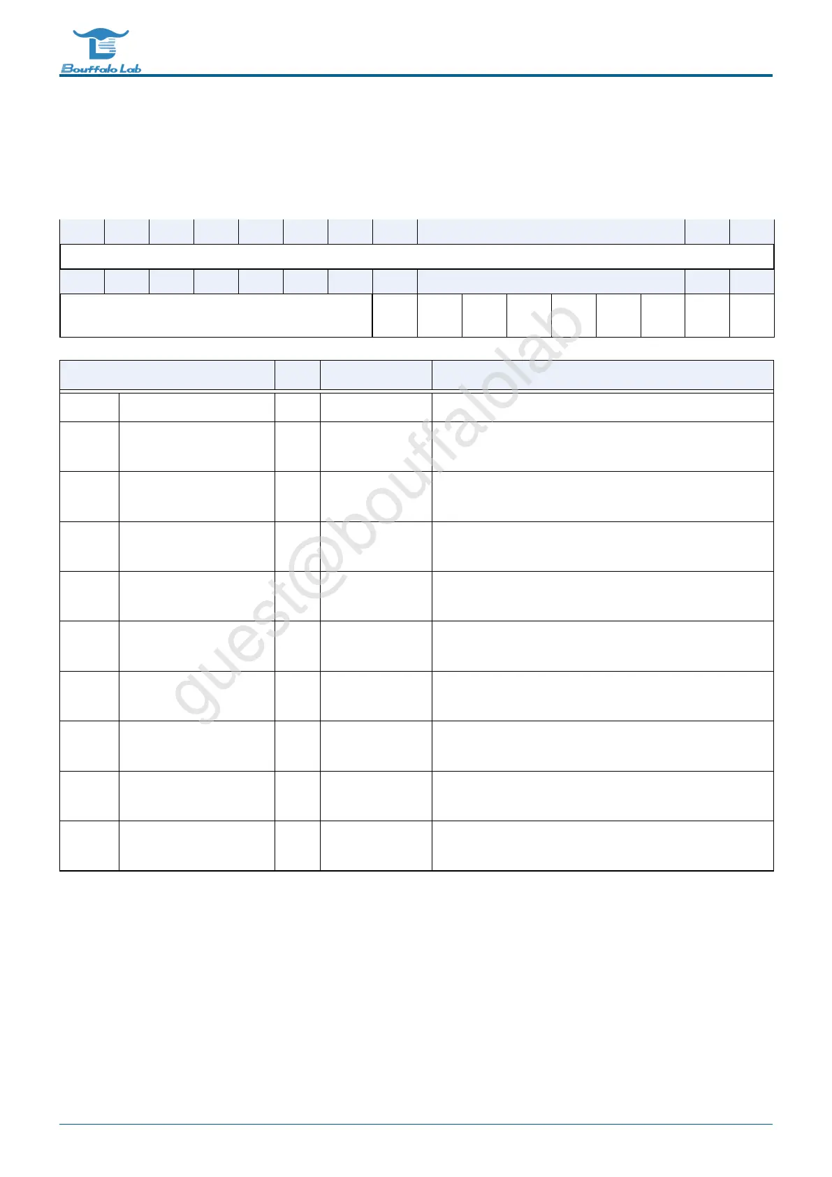
3.3.40 GPIO_CFGCTL35
Address:0x40000194
31 30 29 28 27 26 25 24 23 22 21 20 19 18 17 16
RSVD
15 14 13 12 11 10 9 8 7 6 5 4 3 2 1 0
RSVD GP40
OE
GP39
OE
GP38
OE
GP37
OE
GP36
OE
GP35
OE
GP34
OE
GP33
OE
GP32
OE
Bits
Name Type Reset Description
31:9 RSVD
8 GP40OE R/W 0 Register Controlled GPIO Output Enable (Used when GPIO
Function select to Register Control GPIO)
7 GP39OE R/W 0 Register Controlled GPIO Output Enable (Used when GPIO
Function select to Register Control GPIO)
6 GP38OE R/W 0 Register Controlled GPIO Output Enable (Used when GPIO
Function select to Register Control GPIO)
5 GP37OE R/W 0 Register Controlled GPIO Output Enable (Used when GPIO
Function select to Register Control GPIO)
4 GP36OE R/W 0 Register Controlled GPIO Output Enable (Used when GPIO
Function select to Register Control GPIO)
3 GP35OE R/W 0 Register Controlled GPIO Output Enable (Used when GPIO
Function select to Register Control GPIO)
2 GP34OE R/W 0 Register Controlled GPIO Output Enable (Used when GPIO
Function select to Register Control GPIO)
1 GP33OE R/W 0 Register Controlled GPIO Output Enable (Used when GPIO
Function select to Register Control GPIO)
0 GP32OE R/W 0 Register Controlled GPIO Output Enable (Used when GPIO
Function select to Register Control GPIO)
BL702/704/706 Reference Manual 76/ 375
@2021 Bouffalo Lab