BL702/704/706 Reference Manual
9.3.3 Acceptance filtering function
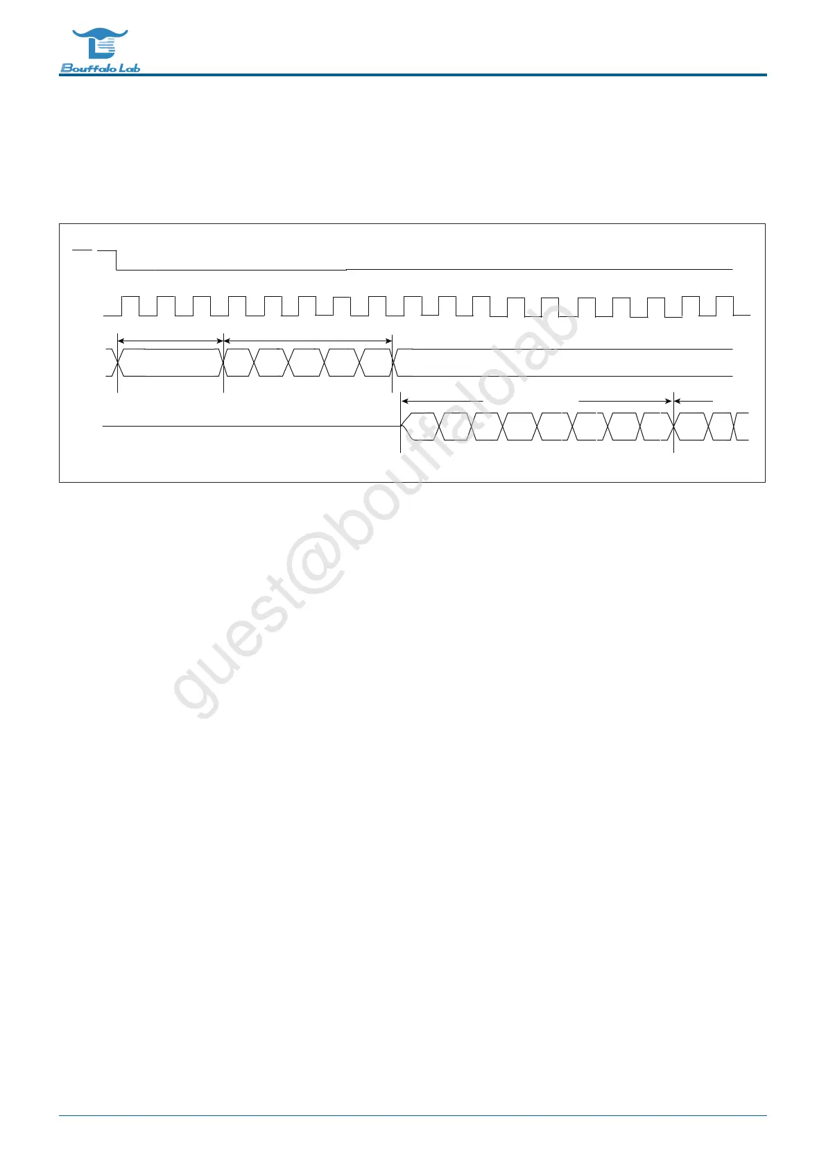
By setting the start and end bits that need to be filtered out, the SPI discards the corresponding data segment in the
received data. As shown below:
CS
High-Impedance State
SO
SI
SCK
Address
Opcode
Dummy Byte
Fig. 9.2: SPI Ignore waveform
In the figure above, the start bit of the filter is set to 0, the end bit is set to 7, the dummy byte is received, and the end
bit is set to 15, the dummy byte is discarded.
9.3.4 Receive error correction
By enabling this function and setting the threshold, the SPI will discard data that does not reach the threshold width.
9.3.5 Slave mode timeout mechanism
By setting a timeout threshold, an interrupt will be triggered when the SPI does not receive a clock signal after ex-
ceeding this time value in slave mode.
9.3.6 I/O transfer mode
The chip communications processor can perform FIFO fill and empty operations in response to interrupts from the
FIFO. Each FIFO has a programmable FIFO trigger threshold to trigger interrupts. When the value in the RX FIFO
exceeds the RX FIFO trigger threshold in the SPI controller 1, an interrupt will be generated and a signal will be sent
to the chip communication processor to clear the RX FIFO. When the value in the TX FIFO is less than or equal to
the TX FIFO trigger threshold in the SPI control register 1 plus 1, an interrupt will be generated and a signal will be
sent to the chip communication processor to refill the TX FIFO.
Query the SPI status register to determine the sampled value in the FIFO and the status of the FIFO. Software is
responsible for ensuring the correct RX FIFO trigger threshold and TX FIFO trigger threshold to prevent receive FIFO
overrun and transmit FIFO underrun.
BL702/704/706 Reference Manual 180/ 375
@2021 Bouffalo Lab