BL702/704/706 Reference Manual
• ADC CH8
• ADC CH9
• ADC CH10
• ADC CH11
• VSSA
• DAC OUTA
• DAC OUTB
• VBAT/2
• TSEN
• VREF
• GND
It should be noted that if VBAT/2 or TSEN is selected as the input signal to be acquired, gpadc_vbat_en or gpadc_-
ts_en needs to be set.
The ADC module can support single-ended input or differential input. If it is single-ended input mode, the negative
input channel needs to select GND.
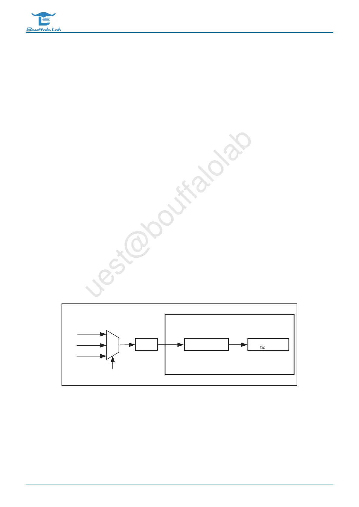
4.3.3 ADC clock
The working clock source of the ADC module is shown in the following figure:
Divider
AUPLL
XCLK
ADC
gpadc_clk_div_radio
gpadc_clk_sel
ADC
Func
onal moudle
f32k_clk
Fig. 4.2: ADC Clock
The ADC clock source can select Audio PLL,XCLK or f32k.The clock source selection is set in the GLB module.While
selecting, the clock source can be divided by the frequency divider.
In general voltage measurement applications, users can choose XCLK as the clock source. In audio applications,
users can use AUPLL to generate common sampling clocks such as 8KHZ and 44.1KHZ. f32k is a low-frequency
clock, which provides a wake-up clock when the MCU sleeps.
BL702/704/706 Reference Manual 93/ 375
@2021 Bouffalo Lab