BL702/704/706 Reference Manual
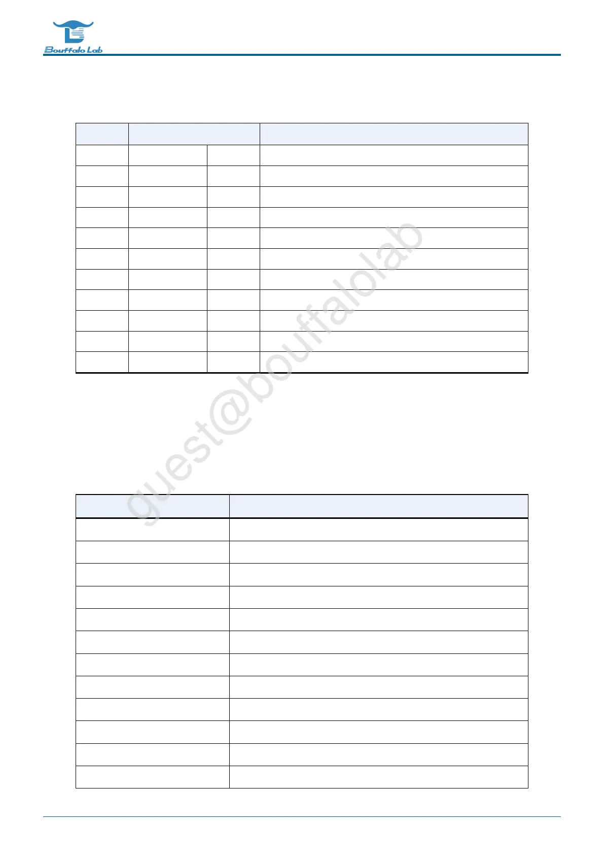
Table 1.2: Memory Map
Module
Base Address Size Description
eFuse 0x40007000 4KB eFuse memory control
SEC 0x40004000 4KB Security engine
GPIP 0x40002000 4KB General purpose DAC/ADC/ACOMP interface control
MIX 0x40001000 4KB Mixed signal register
GLB 0x40000000 4KB Global control register
pSRAM 0x24000000 8MB pSRAM memory
XIP 0x23000000 8MB XIP Flash memory
OCRAM 0x22020000 64KB On-chip memory
DTCM 0x22014000 48KB Data cache memory
ITCM 0x22010000 16KB Instruction cache memory
ROM 0x21000000 192KB Read-only memory
There are 64 interrupt sources. The level or edge trigger is configured by the CPU and can be masked. Details as
follows:
Table 1.3: Interrupt source
Num
Signal source
54~63 wireless
53 brown-out
51~52 hbn_irq
50 pds_int
47~49 wireless
44 gpio_irq
40~42 qdec_int
39 kys_int
35~38 timer_irq
34 pwm_int
32 i2c_int
30 uart1_irq
BL702/704/706 Reference Manual 24/ 375
@2021 Bouffalo Lab