BL702/704/706 Reference Manual
Bits
Name Type Reset Description
7 QDECCSEL R/W 0 QDEC Clock Source Select. 0:xclk 1:f32k (PDS mode)
6:5 RSVD
4:0 QDECCDIV R/W 5’d31 QDEC Clock Divider qdec_clk_sel/(N+1), default 1MHz
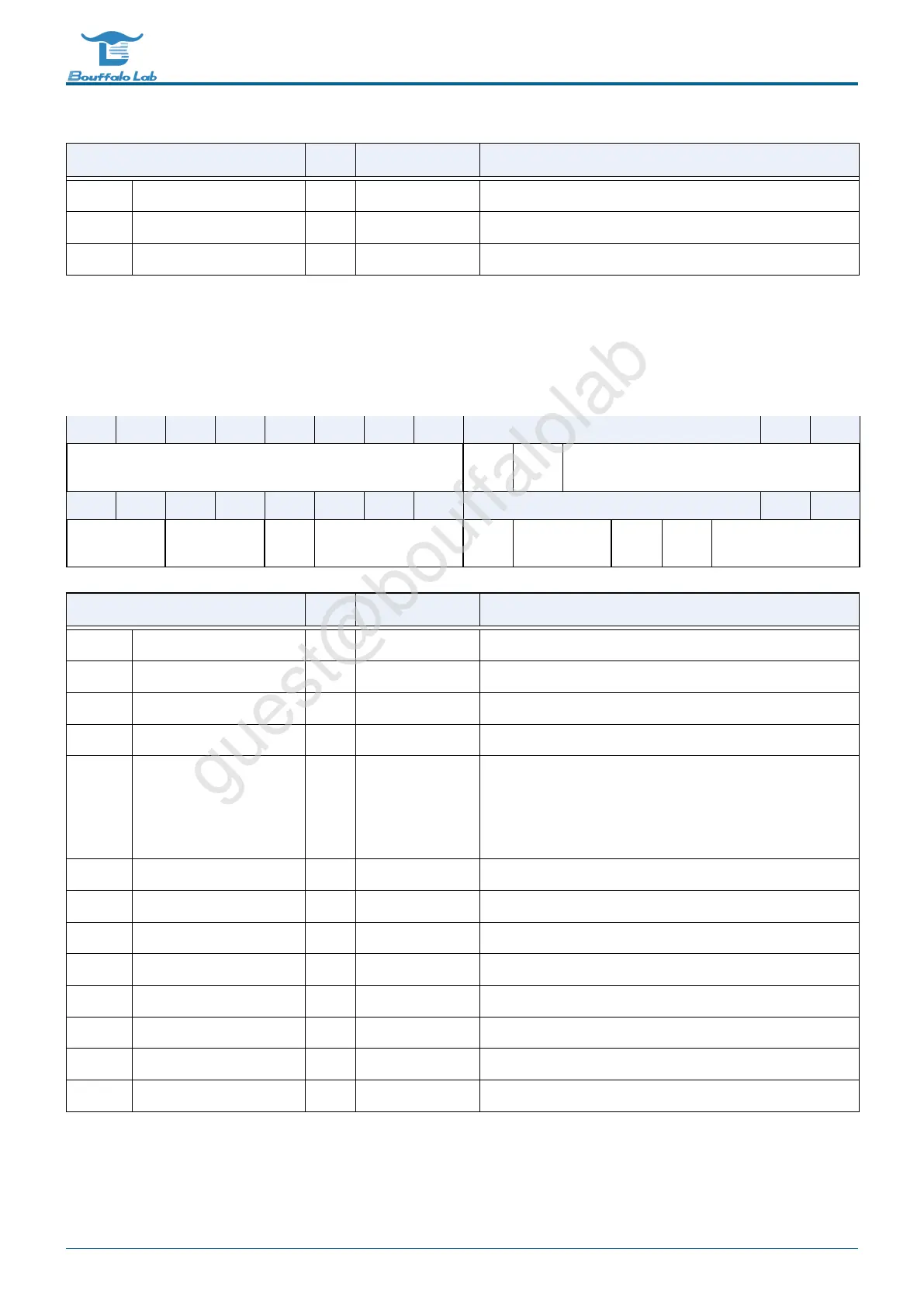
3.3.3 clk_cfg2
Address:0x40000008
31 30 29 28 27 26 25 24 23 22 21 20 19 18 17 16
DMAEN IRCL
EN
RSVD IRCLDIV
15 14 13 12 11 10 9 8 7 6 5 4 3 2 1 0
SFSEL2 SFSEL SFEN SFDIV HUC
SEL
RSVD UART
EN
RSVD UARTDIV
Bits
Name Type Reset Description
31:24 DMAEN R/W 8’hff DMA CH0 7 Clock Enable ; config all 0 if disable DMA
23 IRCLEN R/W 1 IR remote Clock Enable
22 RSVD
21:16 IRCLDIV R/W 6’d15 IR remote Clock Divider xclk(N+1)
15:14 SFSEL2 R/W 0 For sf_clk_sel=0
0: 144MHz
1: xclk
3: 57.6MHz
13:12 SFSEL R/W 2’d2 Flash Clock Select (0:sf_clk_sel2, 1:72M, 2:bclk, 3:96M)
11 SFEN R/W 1 Flash Clock Enable
10:8 SFDIV R/W 3’d3 Flash Clock Divider (Selected Flash Clock)/(N+1)
7 HUCSEL R 0 uart clock selection from HBN (0:fclk 1:96MHz)
6:5 RSVD
4 UARTEN R/W 1 UART Clock Enable
3 RSVD
2:0 UARTDIV R/W 3’d7 UART Clock Divider hbn_uart_clk_sel/(N+1)
BL702/704/706 Reference Manual 42/ 375
@2021 Bouffalo Lab