BL702/704/706 Reference Manual
pushed into the FIFO.
4.3.1 ADC pins and internal signals
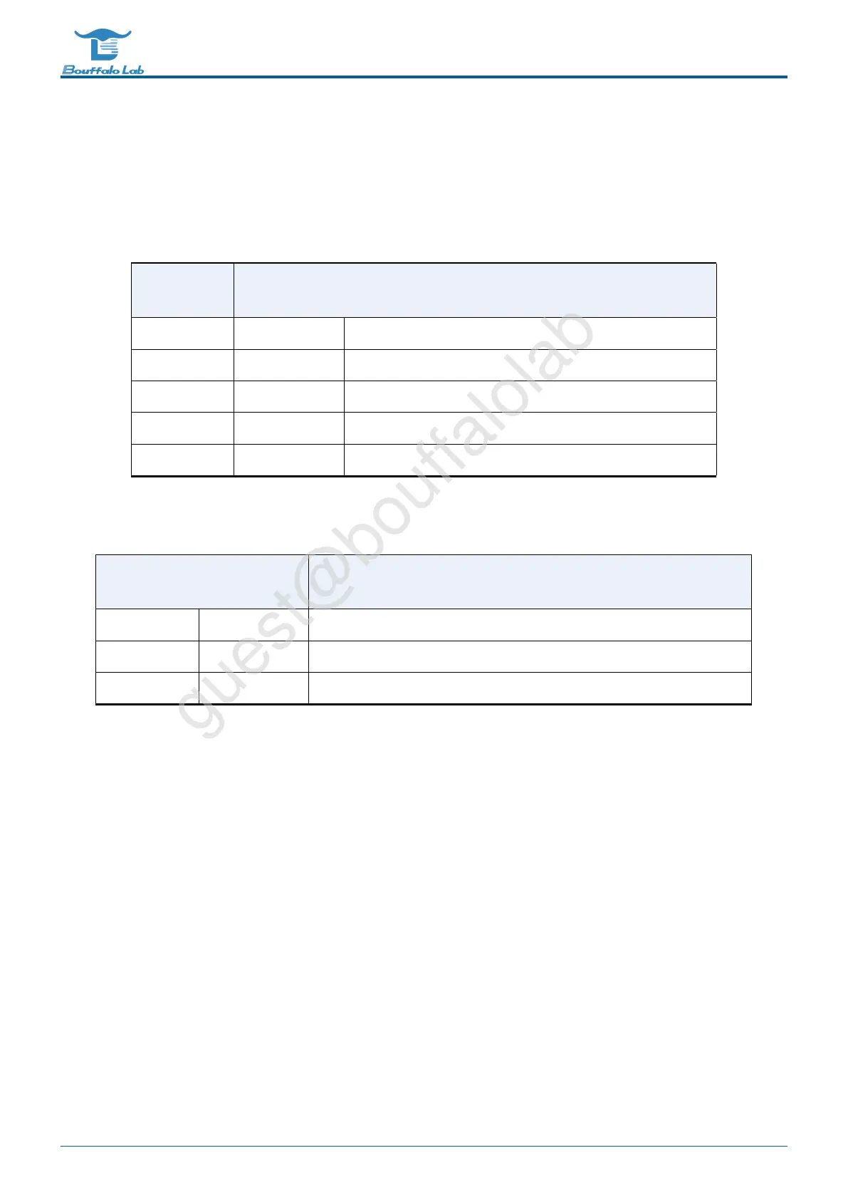
Table 4.1: ADC internal signals
Internal
signals
Signal type Description
VBAT/2 Input Voltage signal divided from the power pin
TSEN Input Internal temperature sensor output voltage
VREF Input Internal analog module reference voltage
DACOUTA Input DAC module output
DACOUTB Input DAC module output
Table 4.2: ADC external pins
External
pins
Signal type Description
VDDA Input Analog power supply and positive reference voltage for the ADC
VSSA Input Ground for analog power supply
ADC_CHX Input 12 analog input channels
4.3.2 ADC channel
The channels that can be selected by the ADC include the input signals of external analog pins and the optional
signals inside the chip:
• ADC CH0
• ADC CH1
• ADC CH2
• ADC CH3
• ADC CH4
• ADC CH5
• ADC CH6
• ADC CH7
BL702/704/706 Reference Manual 92/ 375
@2021 Bouffalo Lab