BL702/704/706 Reference Manual
– 2 DAC internal channels
– 1 VBAT / 2 channel
– 1 TSEN channel
4.3 ADC functional description
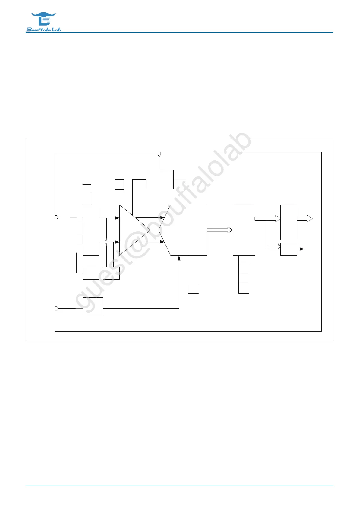
The basic block diagram of the ADC is shown below.
SARADC core
(12bit,max2MHz)
PGA
(2-stage)
MUX
Data
process
Internal
Tsen
VCM_gen
for MIC
Ts
Vbat
Gpdac_a/b
Data_raw[11:0]
IVBIAS
LDO
REF_gen
Pos/neg_sel
Scan
Pga_gain
Diff/single
Clk_div
Res_sel
(12bit/14bit/16bit)
Single/cont mode
Scan(channel info)
DMA
FIFO
PIR
process
Data_final[25:0]
Data_pir[15:2]
Over/under flow
BUS
Interrupt
GPIP_CH[11:0]
CLK
32MHz(max)
VDD33(1.7~3.6V)
Conv_start
Vref_sel
Fig. 4.1: ADC block diagram
The ADC consists of five parts: front-end input channel selector, program-controlled amplifier, ADC sampling module,
data processing module, and FIFO.
The input channel selector is used to select the channel to be sampled. It contains both external analog signals and
internal analog signals. The program-controlled amplifier is used to further process the input signal. It can be set
according to the characteristics of the input signal, such as DC and AC. In order to get more accurate conversion
values.
The ADC sampling module is the most important function module. It obtains the conversion from analog signals
to digital signals through successive comparisons. The conversion result is 12bit. The data processing module is
responsible for further processing the conversion results, including adding channel information. The resulting data is
BL702/704/706 Reference Manual 91/ 375
@2021 Bouffalo Lab