BL702/704/706 Reference Manual
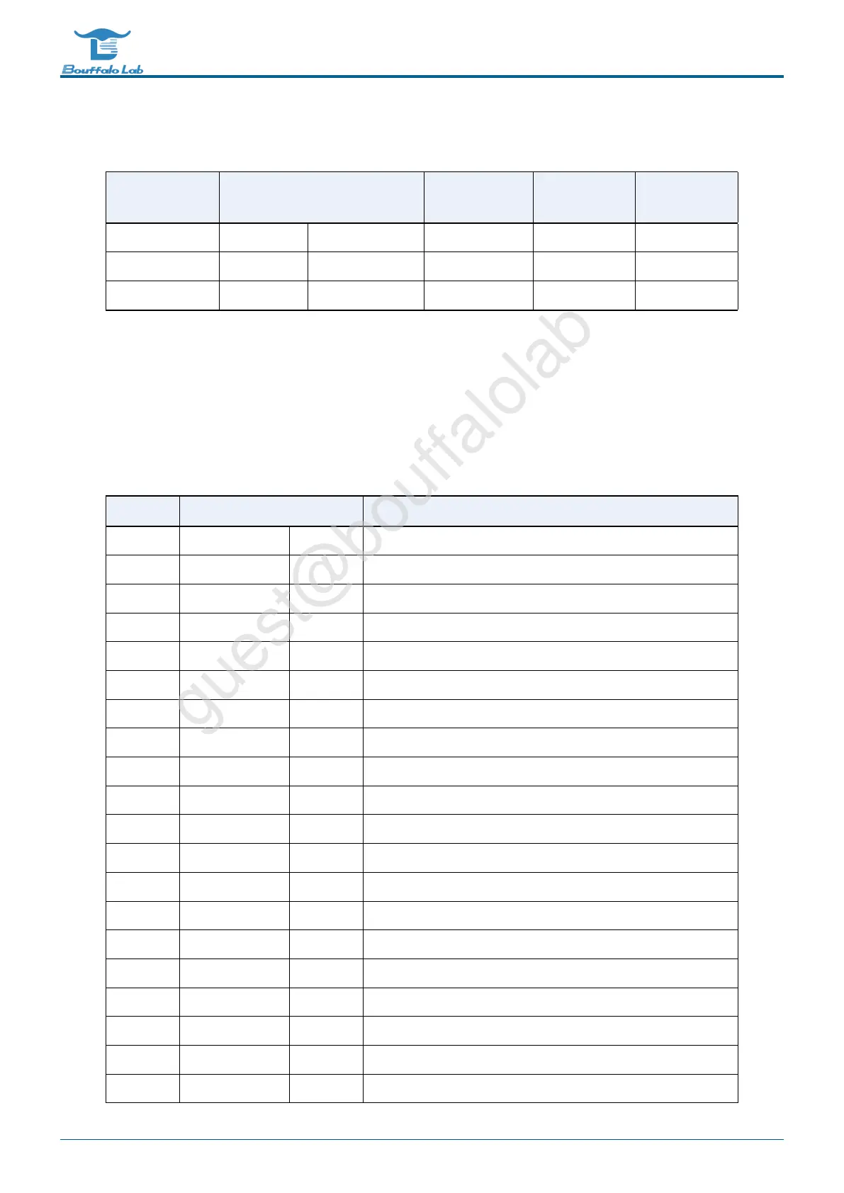
Table 1.1: Bus connection
Slave/Master
CPU Ethernet DMA Encryption
engine
Debug
interface
memory V V V V V
Peripheral V V - V
Zigbee/BLE V - V - V
The address access mainly distinguishes ”memory” or ”peripheral” by [27:24], and the [31:28] bits can be ignored. The
memory space is consecutive addresses 0x2010000~0x202FFFF (128KB SRAM),the read-only memory address is
0x1000000,and the deep sleep memory address is 0x0010000。The off-chip space address is 0x3000000 (maximum
support 8MB Flash). The peripheral space is 0x0000000 ~ 0x000F000.
Table 1.2: Memory Map
Module
Base Address Size Description
RETRAM 0x40010000 4KB Deep sleep memory (Retention RAM)
HBN 0x4000F000 4KB Deep sleep control (Hibernate)
PDS 0x4000E000 4KB Sleep control (Power Down Sleep)
USB 0x4000D800 1KB USB control
EMAC 0x4000D000 2KB Ethernet MAC control
DMA 0x4000C000 4KB DMA control
QSPI 0x4000B000 4KB Flash/pSRAM QSPI control
I2S 0x4000AA00 256B I2S control
KYS 0x4000A900 256B Key-Scan control
QDEC2 0x4000A880 64B Quadrature decoder control
QDEC1 0x4000A840 64B Quadrature decoder control
QDEC0 0x4000A800 64B Quadrature decoder control
IRR 0x4000A600 256B IR Remote control
TIMER 0x4000A500 256B Timer control
PWM 0x4000A400 256B Pulse Width Modulation *5 control
I2C 0x4000A300 256B I2C control
SPI 0x4000A200 256B SPI master/slave control
UART1 0x4000A100 256B UART control (support LIN-bus)
UART0 0x4000A000 256B UART control (support LIN-bus)
L1C 0x40009000 4KB Cache control
BL702/704/706 Reference Manual 23/ 375
@2021 Bouffalo Lab