BL702/704/706 Reference Manual
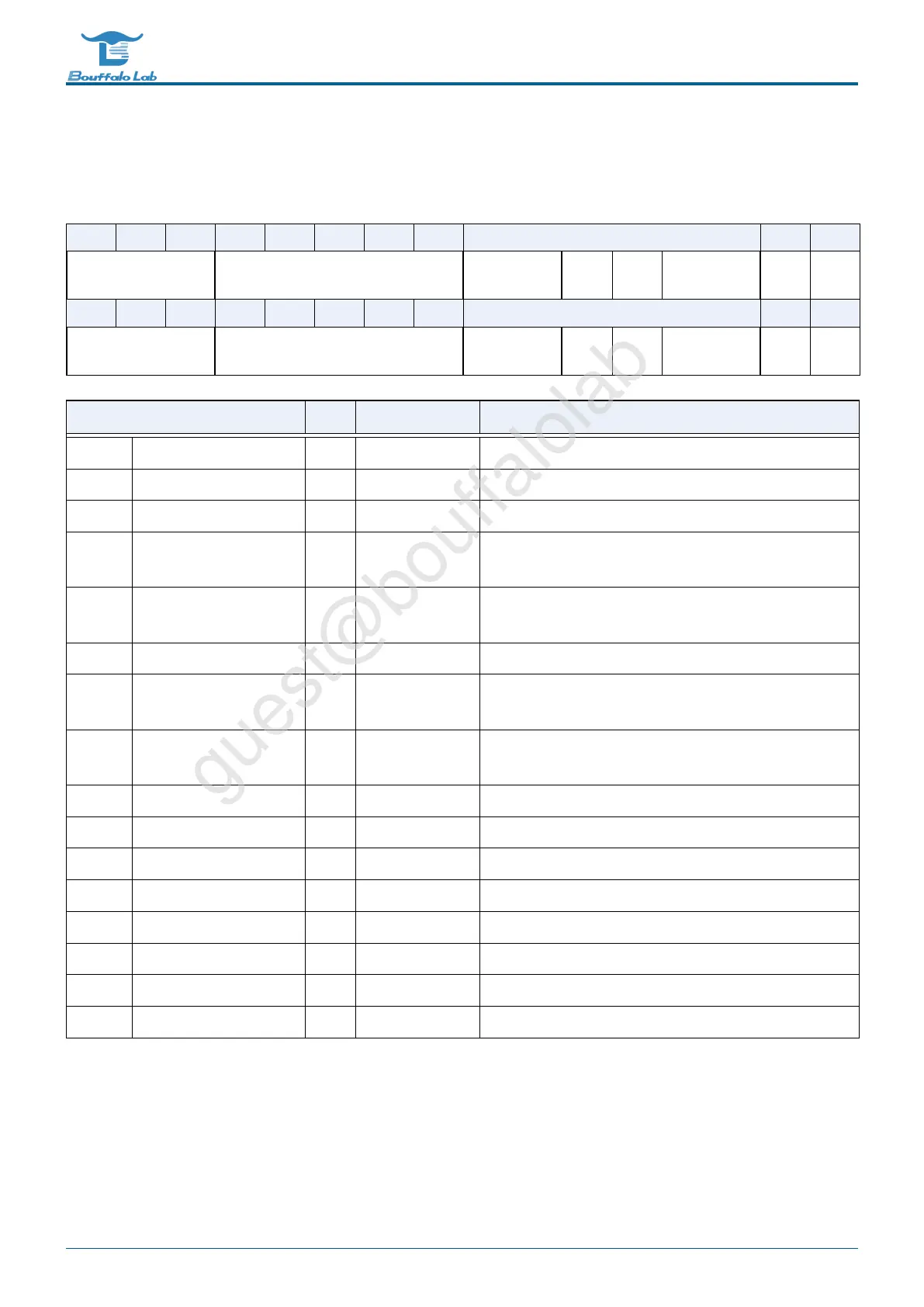
3.3.22 GPIO_CFGCTL4
Address:0x40000110
31 30 29 28 27 26 25 24 23 22 21 20 19 18 17 16
RSVD GP9FUNC RSVD GP9
PD
GP9
PU
GP9DRV GP9
SMT
GP9
IE
15 14 13 12 11 10 9 8 7 6 5 4 3 2 1 0
RSVD GP8FUNC RSVD GP8
PD
GP8
PU
GP8DRV GP8
SMT
GP8
IE
Bits
Name Type Reset Description
31:29 RSVD
28:24 GP9FUNC R/W 5’hE GPIO Function Select (Default : JTAG )
23:22 RSVD
21 GP9PD R/W 0 GPIO Pull Down Control (Use this bit if reg_en_hw_pu_pd
:= 0 (0x4000F014[16])
20 GP9PU R/W 0 GPIO Pull Up Control (Use this bit if reg_en_hw_pu_pd :=
0 (0x4000F014[16])
19:18 GP9DRV R/W 0 GPIO Driving Control
17 GP9SMT R/W 1 GPIO SMT Control(Useless, IE depend on reg_aon_pad_-
ie_smt[0] : 0x4000F014[8])
16 GP9IE R/W 0 GPIO Input Enable (Useless, IE depend on reg_aon_pad_-
ie_smt[0] : 0x4000F014[8])
15:13 RSVD
12:8 GP8FUNC R/W 5’hB GPIO Function Select (Default : SWGPIO )
7:6 RSVD
5 GP8PD R/W 0 GPIO Pull Down Control
4 GP8PU R/W 0 GPIO Pull Up Control
3:2 GP8DRV R/W 0 GPIO Driving Control
1 GP8SMT R/W 1 GPIO SMT Control
0 GP8IE R/W 1 GPIO Input Enable
BL702/704/706 Reference Manual 57/ 375
@2021 Bouffalo Lab