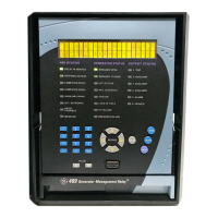
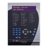
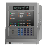
GE Power Management 745 Transformer Management Relay 8-77
8 COMMUNICATIONS 8.3 MODBUS MEMORY MAP
8
xxxx 0000 0101 0001 81 = Logic Input 16
xxxx 0000 0101 0010 82 = Virtual Input 1
xxxx 0000 0101 0011 83 = Virtual Input 2
xxxx 0000 0101 0100 84 = Virtual Input 3
xxxx 0000 0101 0101 85 = Virtual Input 4
xxxx 0000 0101 0110 86 = Virtual Input 5
xxxx 0000 0101 0111 87 = Virtual Input 6
xxxx 0000 0101 1000 88 = Virtual Input 7
xxxx 0000 0101 1001 89 = Virtual Input 8
xxxx 0000 0101 1010 90 = Virtual Input 9
xxxx 0000 0101 1011 91 = Virtual Input 10
xxxx 0000 0101 1100 92 = Virtual Input 11
xxxx 0000 0101 1101 93 = Virtual Input 12
xxxx 0000 0101 1110 94 = Virtual Input 13
xxxx 0000 0101 1111 95 = Virtual Input 14
xxxx 0000 0110 0000 96 = Virtual Input 15
xxxx 0000 0110 0001 97 = Virtual Input 16
xxxx 0000 0110 0010 98 = Output Relay 1
xxxx 0000 0110 0011 99 = Output Relay 2
xxxx 0000 0110 0100 100 = Output Relay 3
xxxx 0000 0110 0101 101 = Output Relay 4
xxxx 0000 0110 0110 102 = Output Relay 5
xxxx 0000 0110 0111 103 = Output Relay 6
xxxx 0000 0110 1000 104 = Output Relay 7
xxxx 0000 0110 1001 105 = Output Relay 8
xxxx 0000 0110 1010 106 = Self-Test Relay
xxxx 0000 0110 1011 107 = Virtual Output 1
xxxx 0000 0110 1100 108 = Virtual Output 2
xxxx 0000 0110 1101 109 = Virtual Output 3
xxxx 0000 0110 1110 110 = Virtual Output 4
xxxx 0000 0110 1111 111 = Virtual Output 5
xxxx 0000 0111 0000 112 = Setpoint Group 1
xxxx 0000 0111 0001 113 = Setpoint Group 2
xxxx 0000 0111 0010 114 = Setpoint Group 3
xxxx 0000 0111 0011 115 = Setpoint Group 4
xxxx 0000 0111 0100 116 = Test Mode
xxxx 0000 0111 0101 117 = Simulation Disabled
xxxx 0000 0111 0110 118 = Simulation Prefault
xxxx 0000 0111 0111 119 = Simulation Fault
xxxx 0000 0111 1000 120 = Simulation Playback
Table 8–7: 745 DATA FORMATS (Sheet 7 of 35)
FORMAT
CODE
APPLICABLE BITS DEFINITION
xxxx 0000 0111 1001 121 = Logic Input Reset
xxxx 0000 0111 1010 122 = Front Panel Reset
xxxx 0000 0111 1011 123 = Comm Port Reset
xxxx 0000 0111 1100 124 = Manual Trace Trigger
xxxx 0000 0111 1101 125 = Auto Trace Trigger
xxxx 0000 0111 1110 126 = Control Power
xxxx 0000 0111 1111 127 = Logic Input Power
xxxx 0000 1000 0000 128 = Analog Output Power
xxxx 0000 1000 0001 129 = Unit Not Calibrated
xxxx 0000 1000 0010 130 = EEPROM Memory
xxxx 0000 1000 0011 131 = Real-Time Clock
xxxx 0000 1000 0100 132 = Battery
xxxx 0000 1000 0101 133 = Emulation Software
xxxx 0000 1000 0110 134 = Int Temperature
xxxx 0000 1000 0111 135 = Flexlogic Equation
xxxx 0000 1000 1000 136 = DSP Processor
xxxx 0000 1000 1001 137 = Bad Xfmr Settings
xxxx 0000 1000 1010 138 = IRIG-B Signal
xxxx 0000 1000 1011 139 = Setpt Access Denied
xxxx 0000 1000 1100 140 = Aging factor Limit
xxxx 0000 1000 1101 141 = Ambient Temperature
xxxx 0000 1000 1110 142 = Tap Changer Failure
F25 16 bits 2's COMPLEMENT SIGNED VALUE,
3 DECIMAL PLACES
Example: –1.234 stored as –1234
F26 16 bits ANALOG OUTPUT RANGE
0000 0000 0000 0000 0 = 0-1 mA
0000 0000 0000 0001 1 = 0-5 mA
0000 0000 0000 0010 2 = 4-20 mA
0000 0000 0000 0011 3 = 0-20 mA
0000 0000 0000 0100 4 = 0-10 mA
F27 16 bits PHASE SEQUENCE
0000 0000 0000 0000 0 = ABC
0000 0000 0000 0001 1 = ACB
F28 16 bits TRANSFORMER TYPE
0000 0000 0000 0000 0 = 2W (extn correction)
0000 0000 0000 0001 1 = Y/y0°
0000 0000 0000 0010 2 = Y/y180°
0000 0000 0000 0011 3 = Y/d30°
0000 0000 0000 0100 4 = Y/d150°
Table 8–7: 745 DATA FORMATS (Sheet 8 of 35)
FORMAT
CODE
APPLICABLE BITS DEFINITION
 Loading...