RS 485 PCI (0602)
514
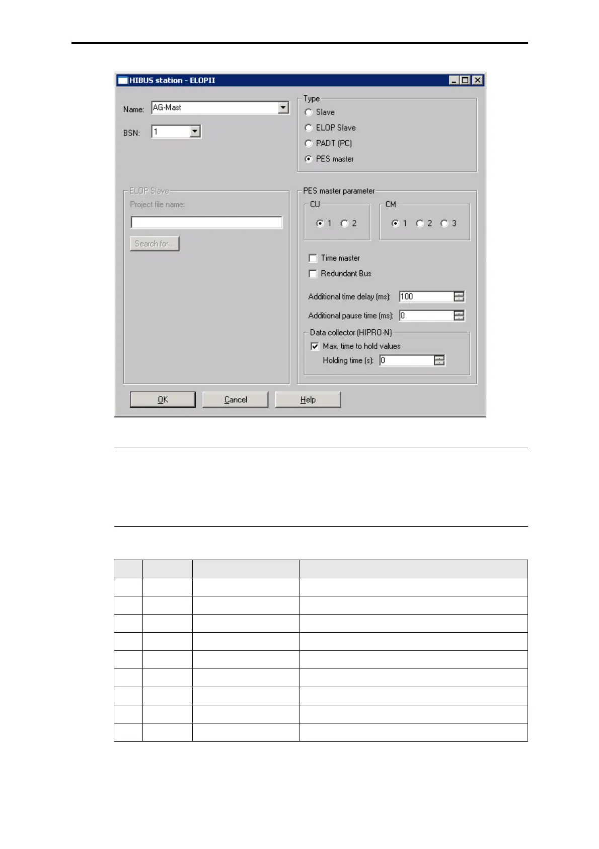
Figure 4: Setting the time delay at PES master
Table 1: Pin assignment of the interfaces RS 485, 9-pole
Note With a loss of the communication connection an increased time delay
triggers an increased bus cycle time. The concerning master waits
during the defined time delay for an answer and so delays the data
exchange.
This performance has to be considered.
Pin RS 485 Signal Meaning
1 - - not used
2 - RP 5 V, decoupled by diodes
3 A/A’ RxD/TxD-A Receive/Transmit Data A
4 - CNTR-A Control signal A
5 C/C’ DGND Data Ground
6 - VP 5 V, positive pole of power supply
7 - - not used
8 B/B’ RxD/TxD-B Receive/Transmit Data B
9 - CNTR-B Control signal B
 Loading...