Equation Reference 5-53
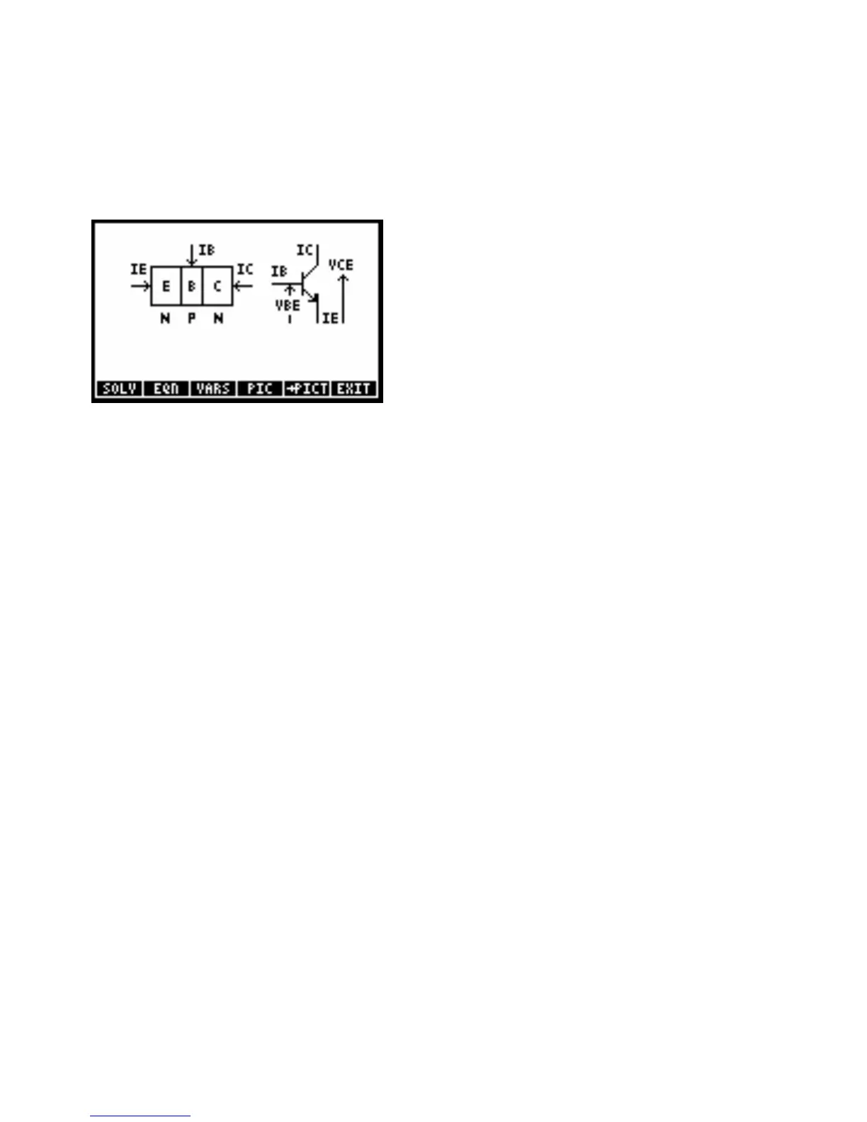
Bipolar Transistors (13, 3)
These equations for an NPN silicon bipolar transistor are based on large-signal models developed by J.J. Ebers
and J.L. Moll. The offset-voltage calculation differs depending on whether the transistor is saturated or not. The
equations also include the special conditions when the emitter-base or collector-base junction is open, which are
convenient for measuring transistor parameters.
Equations:
IS αRIES⋅=
IE IES–e
qVBE⋅
kT⋅
--------------------
1–
⎝⎠
⎜⎟
⎛⎞
⋅αRICS e
qVBE⋅
kT⋅
--------------------
1–
⎝⎠
⎜⎟
⎛⎞
⋅⋅+=
IS αRICS⋅=
IB IE IC++ 0=
IC ICS–e
qVBC⋅
kT⋅
--------------------
1–
⎝⎠
⎜⎟
⎛⎞
⋅αFIES e
qVBE⋅
kT⋅
--------------------
1–
⎝⎠
⎜⎟
⎛⎞
⋅⋅+=
ICO ICS 1 αF αR⋅–()⋅=
ICEO
ICO
1 αF–
----------------
=
VCEsat
kT⋅
q
-----------
LN
1
IC
IB
------
1 αR–()⋅+
αR1
IC
IB
------
1 αF–
αF
----------------
⎝⎠
⎛⎞
⋅–
⎝⎠
⎛⎞
⋅
------------------------------------------------------------
⎝⎠
⎜⎟
⎜⎟
⎜⎟
⎛⎞
⋅=
Example:
Given: IES=1E–5_nA, ICS=2E–5_nA, T=26.85_°C,
α
F=.98,
α
R=.49, IC=1_mA, VBC= –10_V.
Solution: VBE=0.6553_V, IS=0.0000098_nA, ICO=0.000010396_nA, ICEO=0.0005198_nA,
IE= -1.0204_mA, IB=0.0204_mA, VCEsat=0_V.
JFETs (13, 4)
These equations for a silicon N-channel junction field-effect transistor (JFET) are based on the single-sided
step-junction approximation, which assumes the gates are heavily doped compared to the channel doping,. The
drain-current calculation differs depending on whether the gate-junction depletion-layer thickness is less than or
greater than the channel thickness. The equations assume the channel is uniformly doped and end effects (such
as contact, drain, and source resistances) are negligible. (See "SIDENS" in Chapter 3.)