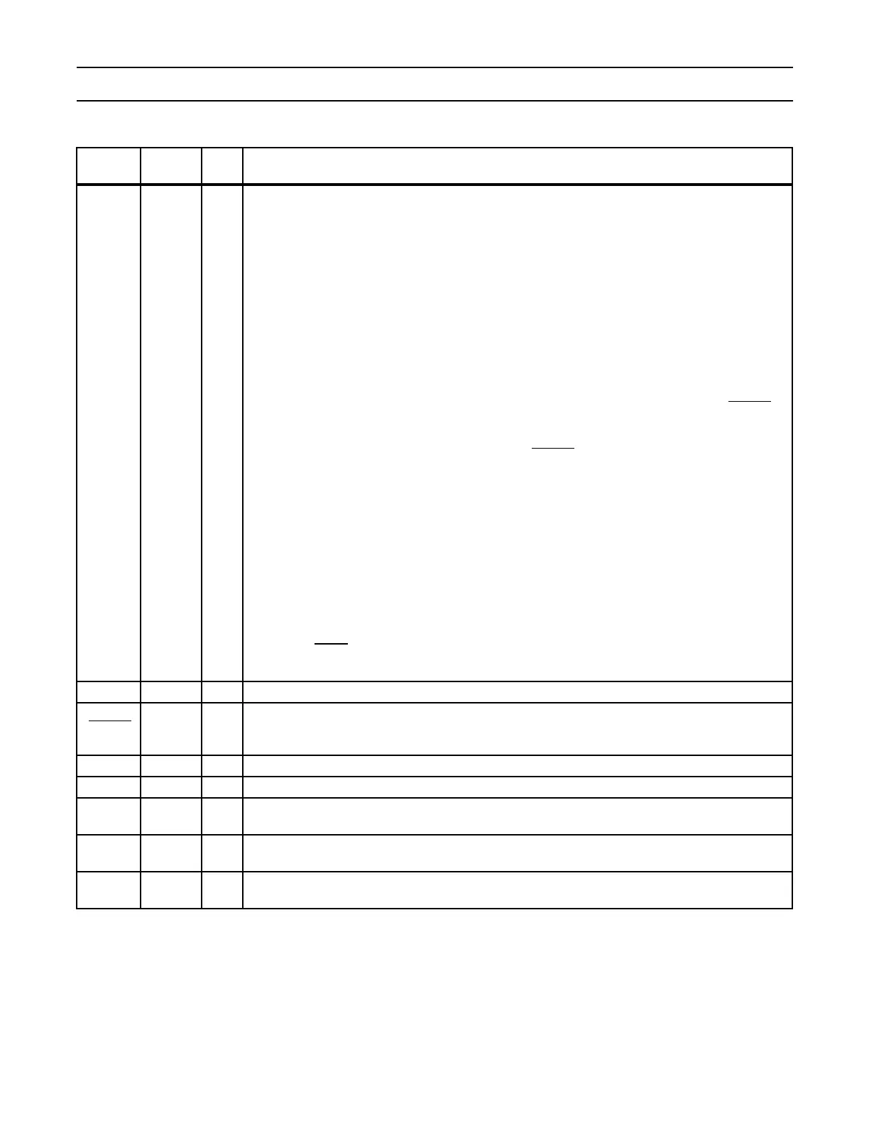
Pin Configuration 114 May 03, 2004
Philips Semiconductors Preliminary User Manual
LPC2119/2129/2194/2292/2294ARM-based Microcontroller
44 O
P1.21 PIPESTAT0 Pipeline Status, bit 0. Standard I/O port with internal pull-up.
40 O
P1.22 PIPESTAT1 Pipeline Status, bit 1. Standard I/O port with internal pull-up.
36 O
P1.23 PIPESTAT2 Pipeline Status, bit 2. Standard I/O port with internal pull-up.
32 O
P1.24 TRACECLK Trace Clock. Standard I/O port with internal pull-up.
28 I
P1.25 EXTIN0 External Trigger Input. Standard I/O with internal pull-up.
24
I/O P1.26 RTCK Returned Test Clock output. Extra signal added to the JTAG port.
Assists debugger synchronization when processor frequency varies.
Bi-directional pin with internal pullup. LOW on this pin while RESET
is
LOW enables pins P1.31:26 to operate as a Debug port after reset.
Important: LOW on pin P1.26 while RESET
is LOW enables pins P1.31:26 to
operate as a Debug port after reset.
64 O
P1.27 TDO Test Data out for JTAG interface.
60 I
P1.28 TDI Test Data in for JTAG interface.
56 I
P1.29 TCK Test Clock for JTAG interface.
52 I
P1.30 TMS Test Mode Select for JTAG interface.
20 I
P1.31 TRST
Test Reset for JTAG interface.
TD1 10 O
TD1:CAN1 transmitter output. Pin is 5 V tolerant with built-in pull-up.
RESET 57 I
External Reset input: A LOW on this pin resets the device, causing I/O ports and peripherals to
take on their default states, and processor execution to begin at address 0. TTL with hysteresis,
5V tolerant.
XTAL1 62 I Input to the oscillator circuit and internal clock generator circuits.
XTAL2 61 O Output from the oscillator amplifier.
V
SS
6, 18, 25,
42, 50
I Ground: 0V reference.
V
SSA
59 I
Analog Ground: 0V reference. This should nominally be the same voltage as V
SS,
but should be
isolated to minimize noise and error.
V
SSA_PLL
58 I
PLL Analog Ground: 0V reference. This should nominally be the same voltage as V
SS,
but
should be isolated to minimize noise and error.
Table 55: Pin description for LPC2119/2129/2194
Pin
Name
LQFP64
Pin #
Type Description