External Memory Controller (EMC) 57 May 03, 2004
Philips Semiconductors Preliminary User Manual
LPC2119/2129/2194/2292/2294ARM-based Microcontroller
PIN DESCRIPTION
REGISTER DESCRIPTION
The external memory controller contains 4 registers as shown in Table 7.
Each register selects the following options for its memory bank:
• The number of idle clock cycles inserted between between read and write accesses in this bank, and between an access in
another bank and an access in this bank, to avoid bus contention between devices (1 to 17 clocks)
• the length of read accesses, except for subsequent reads from a burst ROM (3 to 35 clocks)
• the length of write accesses (3 to 19 clocks)
• whether the bank is write-protected
• whether the bank is 8, 16, or 32 bits wide
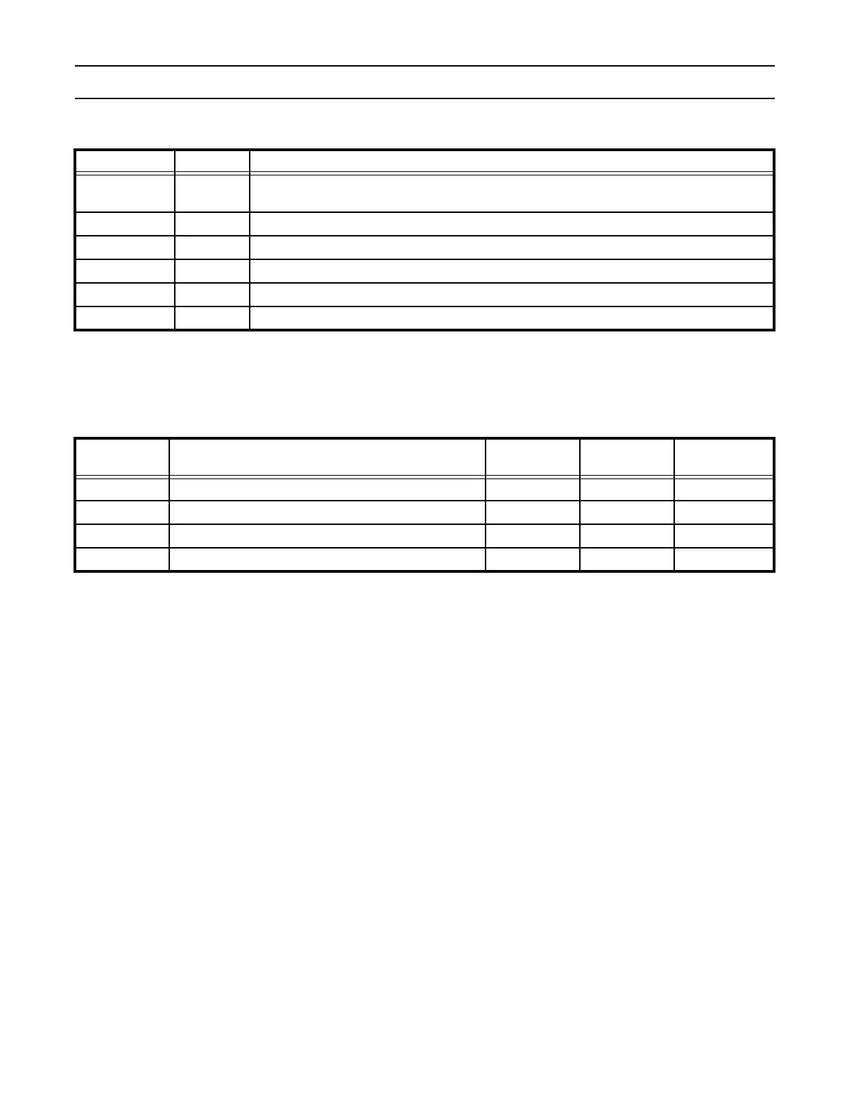
Pin Name Type Pin Description
D[31:0]
Input/
Output
External memory data lines.
A[23:0] Output External memory address lines.
OE Output Low-active Output Enable signal.
BLS[3:0] Output Low-active Byte Lane Select signals.
WE Output Low-active Write Enable signal.
CS[3:0] Output Low-active Chip Select signals.
Table 6: External Memory Controller Pin Description
Name Description Access
Reset Value
(see Table 9)
Address
BCFG0 Configuration register for memory bank 0 Read/Write 0x0000 FBEF 0xFFE00000
BCFG1 Configuration register for memory bank 1 Read/Write 0x2000 FBEF 0xFFE00004
BCFG2 Configuration register for memory bank 2 Read/Write 0x1000 FBEF 0xFFE00008
BCFG3 Configuration register for memory bank 3 Read/Write 0x0000 FBEF 0xFFE0000C
Table 7: External Memory Controller Register Map