Timer0 and Timer1 222 May 03, 2004
Philips Semiconductors Preliminary User Manual
LPC2119/2129/2194/2292/2294ARM-based Microcontroller
ARCHITECTURE
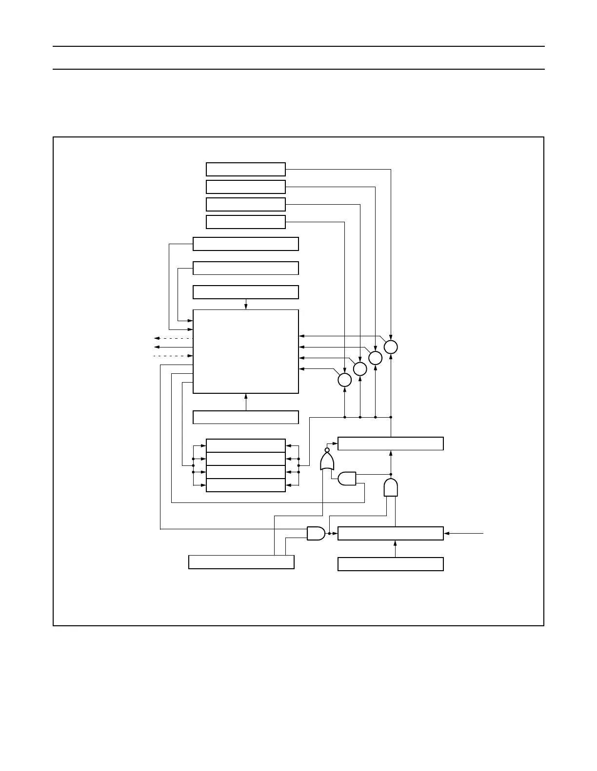
The block diagram for TIMER0 and TIMER1 is shown in Figure 41.
Figure 41: Timer block diagram
=
=
Match Register 0
Match Register 1
Match Register 2
Match Register 3
=
Prescale Register
MAXVAL
Prescale Counter
Timer Counter
Timer Control Register
Capture Control Register
Match Control Register
External Match Register
Interrupt Register
TCI
ENABLERESET
CE
CSN
MAT[3:0]
Interrupt
CAP[3:0]
Stop on Match
Reset on Match
Load[3:0]
Control
=
Capture Register 0
Capture Register 1
Capture Register 2
Capture Register 3*
* Note that Capture Register 3 cannot be used on TIMER0
pclk