Pin Connect Block 126 May 03, 2004
Philips Semiconductors Preliminary User Manual
LPC2119/2129/2194/2292/2294ARM-based Microcontroller
8. PIN CONNECT BLOCK
FEATURES
• Allows individual pin configuration
APPLICATIONS
The purpose of the Pin Connect Block is to configure the microcontroller pins to the desired functions.
DESCRIPTION
The pin connect block allows selected pins of the microcontroller to have more than one function. Configuration registers control
the multiplexers to allow connection between the pin and the on chip peripherals.
Peripherals should be connected to the appropriate pins prior to being activated, and prior to any related interrupt(s) being
enabled. Activity of any enabled peripheral function that is not mapped to a related pin should be considered undefined.
Selection of a single function on a port pin completely excludes all other functions otherwise available on the same pin.
The only partial exception from the above rule of exclusion is the case of inputs to the A/D converter. Regardless of the function
that is selected for the port pin that also hosts the A/D input, this A/D input can be read at any time and variations of the voltage
level on this pin will be reflected in the A/D readings. However, valid analog reading(s) can be obtained if and only if the function
of an analog input is selected. Only in this case proper interface circuit is active in between the physical pin and the A/D module.
In all other cases, a part of digital logic necessary for the digital function to be performed will be active, and will disrupt proper
behavior of the A/D.
REGISTER DESCRIPTION
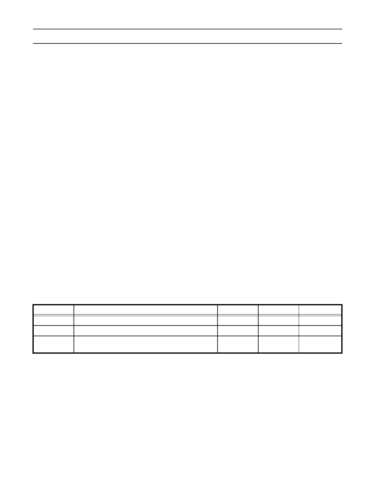
The Pin Control Module contains 2 registers as shown in Table 57. below.
Table 57: Pin Connect Block Register Map
Name Description Access Reset Value Address
PINSEL0 Pin function select register 0 Read/Write 0x0000 0000 0xE002C000
PINSEL1 Pin function select register 1 Read/Write 0x1540 0000 0xE002C004
PINSEL2 Pin function select register 2 Read/Write
See Table 63
and Table 64
0xE002C014
 Loading...