A/D Converter 238 May 03, 2004
Philips Semiconductors Preliminary User Manual
ARM-based Microcontroller
LPC2119/2129/2194/2292/2294
17. A/D CONVERTER
FEATURES
• 10 bit successive approximation analog to digital converter.
• Input multiplexing among 4 pins (LPC2119/2129/2194) or 8 pins (LPC2292/2294)
• Power down mode
• Measurement range 0 to 3 V
• 10 bit conversion time >= 2.44 uS
• Burst conversion mode for single or multiple inputs
• Optional conversion on transition on input pin or Timer Match signal
DESCRIPTION
Basic clocking for the A/D converter is provided by the VPB clock. A programmable divider is included to scale this clock to the
4.5 MHz (max) clock needed by the successive approximation process. A fully accurate conversion requires 11 of these clocks.
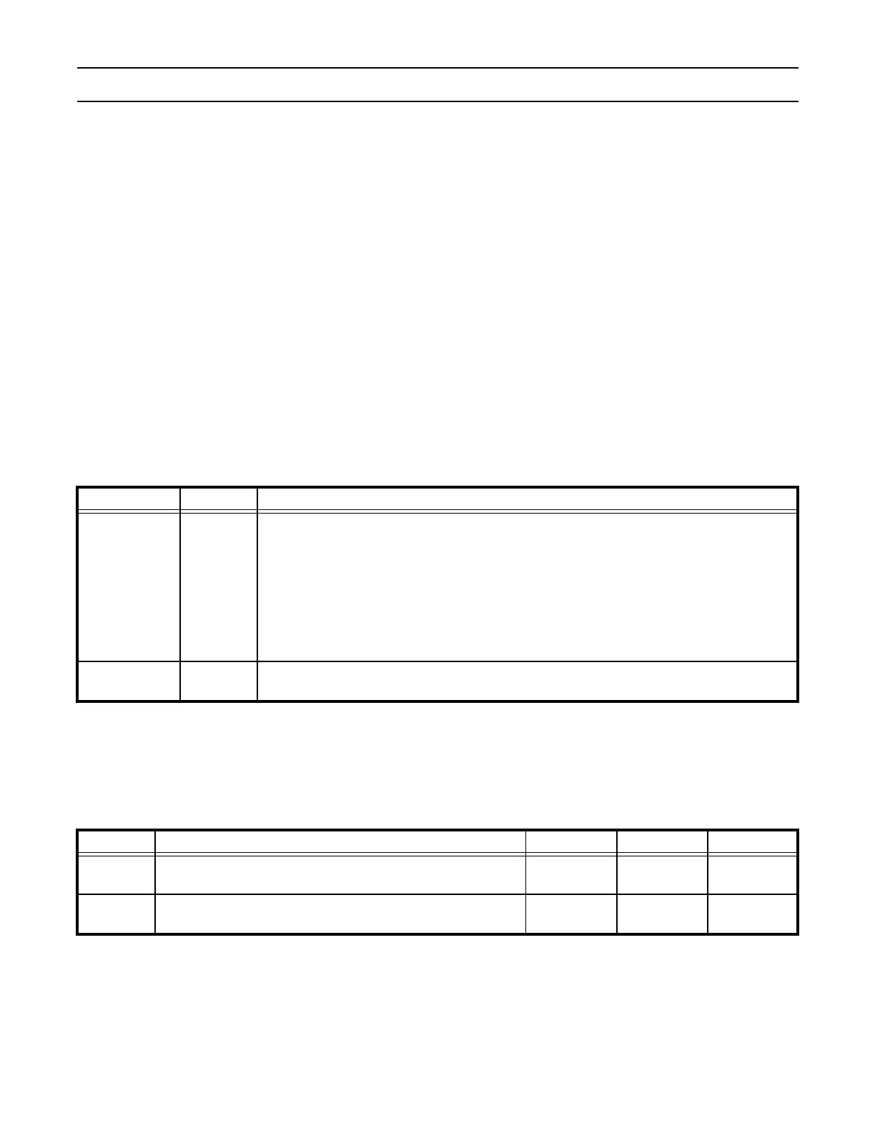
PIN DESCRIPTIONS
REGISTER DESCRIPTION
The base address of the A/D Converter is 0xE003 4000 (page 51). The A/D Converter includes 2 registers as shown in Table
173.
Table 172: A/D Pin Description
Pin Name Type Pin Description
Ain7:0 Input
Analog Inputs. The A/D converter cell can measure the voltage on any of these 8 input signals,
but the 64-pin packages restrict the choice to Ain3:0. Note that these analog inputs are always
connected to their pins, even if the Pin Multiplexing Register assigns them to port pins. A
simple self-test of the A/D Converter can be done by driving these pins as port outputs.
Note: if the A/D converter is used, signal levels on analog input pins must not be above the
level of V
3A
at any time. Otherwise, A/D converter readings will be invalid. If the A/D converter
is not used in an application then the pins associated with A/D inputs can be used as 5V tolerant
digital IO pins.
V
3A
, V
SSA
Power
Analog Power and Ground. These should be nominally the same voltages as V
3
and V
SSD
,
but should be isolated to minimize noise and error.
Table 173: A/D Registers
Name Description Access Reset Value Address
ADCR
A/D Control Register. The ADCR register must be written to
select the operating mode before A/D conversion can occur.
Read/Write 0x0000 0001 0xE003 4000
ADDR
A/D Data Register. This register contains the ADC’s DONE bit
and (when DONE is 1) the 10-bit result of the conversion.
Read/Write NA 0xE003 4004