Timer0 and Timer1 216 May 03, 2004
Philips Semiconductors Preliminary User Manual
LPC2119/2129/2194/2292/2294ARM-based Microcontroller
REGISTER DESCRIPTION
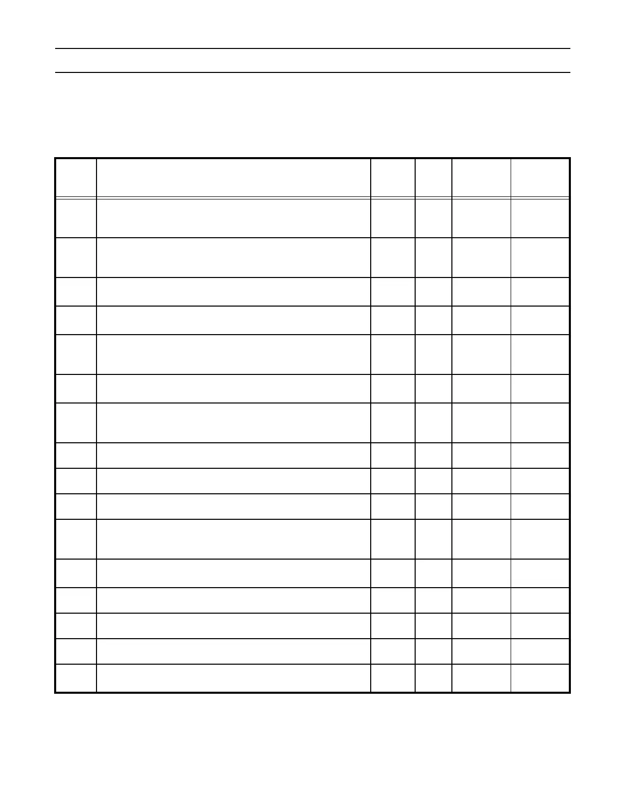
Each Timer contains the registers shown in Table 157. More detailed descriptions follow.
*Reset Value refers to the data stored in used bits only. It does not include reserved bits content.
Table 157: TIMER0 and TIMER1 Register Map
Generic
Name
Description Access
Reset
Value*
TIMER0
Address &
Name
TIMER1
Address &
Name
IR
Interrupt Register. The IR can be written to clear interrupts. The IR
can be read to identify which of eight possible interrupt sources are
pending.
R/W 0
0xE0004000
T0IR
0xE0008000
T1IR
TCR
Timer Control Register. The TCR is used to control the Timer
Counter functions. The Timer Counter can be disabled or reset
through the TCR.
R/W 0
0xE0004004
T0TCR
0xE0008004
T1TCR
TC
Timer Counter. The 32-bit TC is incremented every PR+1 cycles of
pclk. The TC is controlled through the TCR.
RW 0
0xE0004008
T0TC
0xE0008008
T1TC
PR
Prescale Register. The TC is incremented every PR+1 cycles of
pclk.
R/W 0
0xE000400C
T0PR
0xE000800C
T1PR
PC
Prescale Counter. The 32-bit PC is a counter which is incremented
to the value stored in PR. When the value in PR is reached, the TC
is incremented.
R/W 0
0xE0004010
T0PC
0xE0008010
T1PC
MCR
Match Control Register. The MCR is used to control if an interrupt
is generated and if the TC is reset when a Match occurs.
R/W 0
0xE0004014
T0MCR
0xE0008014
T1MCR
MR0
Match Register 0. MR0 can be enabled through the MCR to reset
the TC, stop both the TC and PC, and/or generate an interrupt
every time MR0 matches the TC.
R/W 0
0xE0004018
T0MR0
0xE0008018
T1MR0
MR1 Match Register 1. See MR0 description. R/W 0
0xE000401C
T0MR1
0xE000801C
T1MR1
MR2 Match Register 2. See MR0 description. R/W 0
0xE0004020
T0MR2
0xE0008020
T1MR2
MR3 Match Register 3. See MR0 description. R/W 0
0xE0004024
T0MR3
0xE0008024
T1MR3
CCR
Capture Control Register. The CCR controls which edges of the
capture inputs are used to load the Capture Registers and whether
or not an interrupt is generated when a capture takes place.
R/W 0
0xE0004028
T0CCR
0xE0008028
T1CCR
CR0
Capture Register 0. CR0 is loaded with the value of TC when there
is an event on the CAP0.0(CAP1.0) input.
RO 0
0xE000402C
T0CR0
0xE000802C
T1CR0
CR1 Capture Register 1. See CR0 description. RO 0
0xE0004030
T0CR1
0xE0008030
T1CR1
CR2 Capture Register 2. See CR0 description. RO 0
0xE0004034
T0CR2
0xE0008034
T1CR2
CR3 Capture Register 3. See CR0 description. RO 0
0xE0004038
T0CR3
0xE0008038
T1CR3
EMR
External Match Register. The EMR controls the external match pins
MAT0.0-3 (MAT1.0-3).
R/W 0
0xE000403C
T0EMR
0xE000803C
T1EMR