Pin Connect Block 127 May 03, 2004
Philips Semiconductors Preliminary User Manual
LPC2119/2129/2194/2292/2294ARM-based Microcontroller
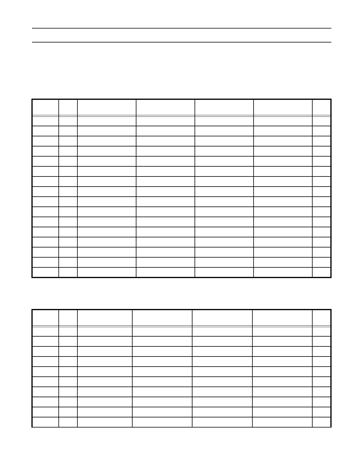
Pin Function Select Register 0 (PINSEL0 - 0xE002C000)
The PINSEL0 register controls the functions of the pins as per the settings listed in Table 65. The direction control bit in the
IO0DIR register is effective only when the GPIO function is selected for a pin. For other functions, direction is controlled
automatically.
Table 58: Pin Function Select Register 0 for LPC2119/2129/2292 (PINSEL0 - 0xE002C000)
PINSEL0
Pin
Name
Function when 00 Function when 01 Function when 10 Function when 11
Reset
Value
1:0 P0.0 GPIO Port 0.0 TxD (UART0) PWM1 Reserved 00
3:2 P0.1 GPIO Port 0.1 RxD (UART0) PWM3 EINT0 00
5:4 P0.2 GPIO Port 0.2 SCL (I
2
C) Capture 0.0 (TIMER0) Reserved 00
7:6 P0.3 GPIO Port 0.3 SDA (I
2
C) Match 0.0 (TIMER0) EINT1 00
9:8 P0.4 GPIO Port 0.4 SCK (SPI0) Capture 0.1 (TIMER0) Reserved 00
11:10 P0.5 GPIO Port 0.5 MISO (SPI0) Match 0.1 (TIMER0) Reserved 00
13:12 P0.6 GPIO Port 0.6 MOSI (SPI0) Capture 0.2 (TIMER0) Reserved 00
15:14 P0.7 GPIO Port 0.7 SSEL (SPI0) PWM2 EINT2 00
17:16 P0.8 GPIO Port 0.8 TxD UART1 PWM4 Reserved 00
19:18 P0.9 GPIO Port 0.9 RxD (UART1) PWM6 EINT3 00
21:20 P0.10 GPIO Port 0.10 RTS (UART1) Capture 1.0 (TIMER1) Reserved 00
23:22 P0.11 GPIO Port 0.11 CTS (UART1) Capture 1.1 (TIMER1) Reserved 00
25:24 P0.12 GPIO Port 0.12 DSR (UART1) Match 1.0 (TIMER1) Reserved 00
27:26 P0.13 GPIO Port 0.13 DTR (UART1) Match 1.1 (TIMER1) Reserved 00
29:28 P0.14 GPIO Port 0.14 CD (UART1) EINT1 Reserved 00
31:30 P0.15 GPIO Port 0.15 RI (UART1) EINT2 Reserved 00
Table 59: Pin Function Select Register 0 for LPC2194/2294 (PINSEL0 - 0xE002C000)
PINSEL0
Pin
Name
Function when 00 Function when 01 Function when 10 Function when 11
Reset
Value
1:0 P0.0 GPIO Port 0.0 TxD (UART0) PWM1 Reserved 00
3:2 P0.1 GPIO Port 0.1 RxD (UART0) PWM3 EINT0 00
5:4 P0.2 GPIO Port 0.2 SCL (I
2
C) Capture 0.0 (TIMER0) Reserved 00
7:6 P0.3 GPIO Port 0.3 SDA (I
2
C) Match 0.0 (TIMER0) EINT1 00
9:8 P0.4 GPIO Port 0.4 SCK (SPI0) Capture 0.1 (TIMER0) Reserved 00
11:10 P0.5 GPIO Port 0.5 MISO (SPI0) Match 0.1 (TIMER0) Reserved 00
13:12 P0.6 GPIO Port 0.6 MOSI (SPI0) Capture 0.2 (TIMER0) Reserved 00
15:14 P0.7 GPIO Port 0.7 SSEL (SPI0) PWM2 EINT2 00
17:16 P0.8 GPIO Port 0.8 TxD UART1 PWM4 Reserved 00
19:18 P0.9 GPIO Port 0.9 RxD (UART1) PWM6 EINT3 00