Introduction 20 May 03, 2004
Philips Semiconductors Preliminary User Manual
LPC2119/2129/2194/2292/2294ARM-based Microcontroller
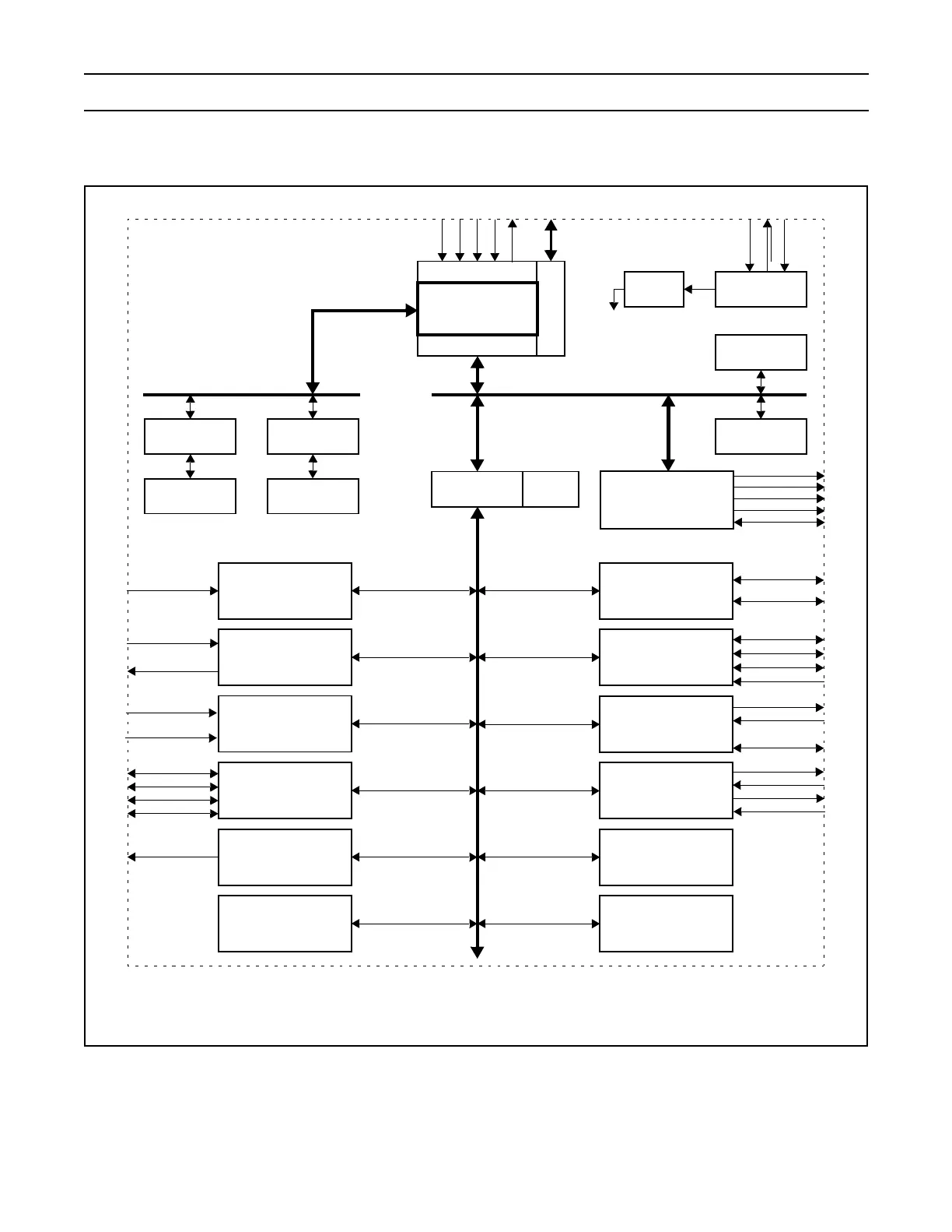
BLOCK DIAGRAM
Figure 1: LPC2119/2129/2194/2292/2294 Block Diagram
Internal SRAM
Controller
AHB
Decoder
Internal Flash
Controller
ARM7TDMI-S
16 kB
SRAM
128/256 kB
FLASH
I
2
C Serial
Interface
Vectored Interrupt
Controller
* Shared with GPIO
1
When Test/Debug Interface is used, GPIO/other functions sharing these pins are not available
2
LPC2292/2294 only.
3
LPC2194/2294 only.
AMBA AHB
(Advanced High-performance Bus)
VPB (VLSI
Peripheral Bus)
Test/Debug Interface
TDO
1
TRST
1
TMS
1
TDI
1
TCK
1
AHB Bridge
System
Functions
Xtal2
RESET
Xtal1
Emulation Trace
Module
SCL
SDA
SPI Serial
Interfaces 0 & 1
SCK0,1
MOSI0,1
MISO0,1
SSEL0,1
UART 0 & 1
TxD0,1
RxD0,1
Ain3:0
A/D
Converter
Real Time
Clock
P0.30:0
General
Purpose I/O
PWM6:1
PWM0
8 x CAP0
8 x MAT
Capture /
Compare
TIMER 0 & 1
Watchdog
Timer
DSR1,CTS1,D
CD1, RI1
PLL
AHB to VPB
Bridge
System
Clock
System
Control
VPB
Divider
EINT3:0
External
Interrupts
ARM7 Local Bus
External Memory
Controller
2
BLS3:0*
OE, WE*
D31:0*
A23:0*
CS3:0*
P1.31:16, 1:0
2
P2.31:0
2
P3.31:0
2
Ain7:4
2
CAN
TD2,1
RD2,1
TD4:3
3
RD4,3
3