CAN Controllers and Acceptance Filter 189 May 03, 2004
Philips Semiconductors Preliminary User Manual
LPC2119/2129/2292/2294ARM-based Microcontroller
PIN DESCRIPTION
MEMORY MAP OF THE CAN BLOCK
The CAN Controllers and Acceptance Filter occupy a number of VPB slots, as follows:
CAN CONTROLLER REGISTERS
CAN block implements the registers shown in Table 123 and 124. More detailed descriptions follow.
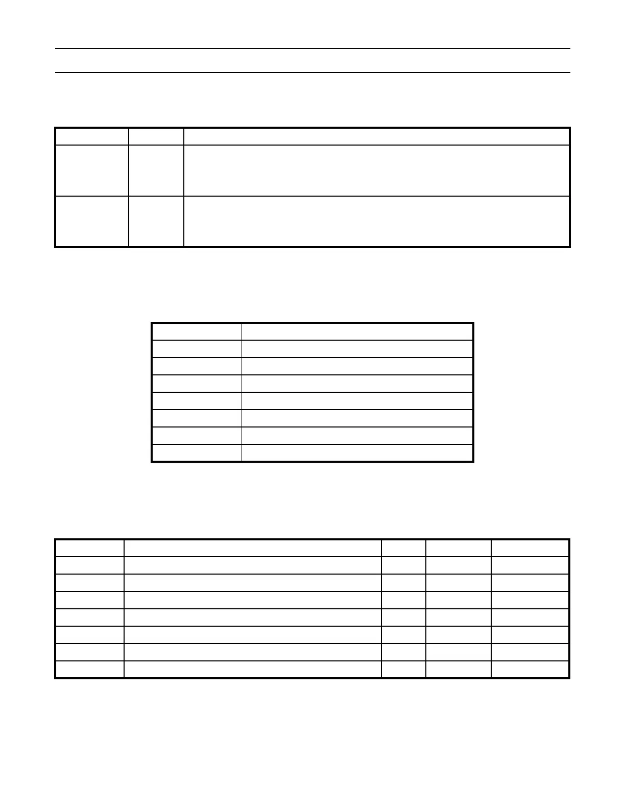
Table 121: CAN Pin Descriptions
Pin Name Type Description
RX4-1 Inputs
Serial Inputs. From CAN transceivers.
Note: RX2 and RX1 are available in all parts having CAN module(s). RX4 and RX3 are
available in LPC2194/2294 only.
TX4-1 Outputs
Serial Outputs. To CAN transceivers.
Note: TX2 and TX1 are available in all parts having CAN module(s). TX4 and TX3 are available
in LPC2194/2294 only.
Table 122: Memory Map of the CAN Block
Address Range Used For
E003 8000 - 87FF Acceptance Filter RAM
E003 C000 - C017 Acceptance Filter Registers
E004 0000 - 000B Central CAN Registers
E004 4000 - 405F CAN Controller 1 Registers
E004 8000 - 805F CAN Controller 2 Registers
E004 C000 - C05F CAN Controller 3 Registers (LPC2194/2294 only)
E005 0000 - 005F CAN Controller 4 Registers (LPC2194/2294 only)
Table 123: CAN Acceptance Filter and Central CAN Registers
Name Description Access Reset Value Address
AFMR Acceptance Filter Register R/W 1 0xE003 C000
SFF_sa Standard Frame Individual Start Address Register R/W 0 0xE003 C004
SFF_GRP_sa Standard Frame Group Start Address Register R/W 0 0xE003 C008
EFF_sa Extended Frame Start Address Register R/W 0 0xE003 C00C
EFF_GRP_sa Extended Frame Group Start Address Register R/W 0 0xE003 C010
ENDofTable End of AF Tables register R/W 0 0xE003 C014
LUTerrAd LUT Error Address register RO 0 0xE003 C018