GPIO 137 May 03, 2004
Philips Semiconductors Preliminary User Manual
LPC2119/2129/2194/2292/2294ARM-based Microcontroller
(IO0CLR - 0xE002800C, IO1CLR - 0xE002801C, IO2CLR - 0xE002802C, IO3CLR - 0xE002803C)
This register is used to produce a LOW level at port pins if they are configured as GPIO in an OUTPUT mode. Writing 1 produces
a LOW level at the corresponding port pins and clears the corresponding bits in the IOSET register. Writing 0 has no effect. If
any pin is configured as an input or a secondary function, writing to IOCLR has no effect.
GPIO Direction Register
(IO0DIR - 0xE0028008, IO1DIR - 0xE0028018, IO2DIR - 0xE0028028, IO3DIR - 0xE0028038)
This register is used to control the direction of the pins when they are configured as GPIO port pins. Direction bit for any pin must
be set according to the pin functionality.
GPIO USAGE NOTES
If for the specified output pin corresponding bit is set both in GPIO Output Set Register (IOnSET) and in GPIO Output Clear
Register (IOnCLR), observed pin will output level determined by the later write access of IOnSET nad IOnCLR. This means that
in case of sequence:
IO0SET = 0x0000 0080
IO0CLR = 0x0000 0080
pin P0.7 will have low output, since access to Clear register came after access to Set register.
Applications that require instanatneous appearance of zeros and ones on the respected parallel port can use direct access to
port’s corresponding GPIO Pin Value Register (IOPIN).
Assuming that pins P0.8 to P0.15 are configured as output, write to IO0PIN:
IO0PIN = 0x0000 C700
will produce the same output as following sequence of writes:
IO0SET = 0x0000 C700
IO0CLR = 0x0000 3800
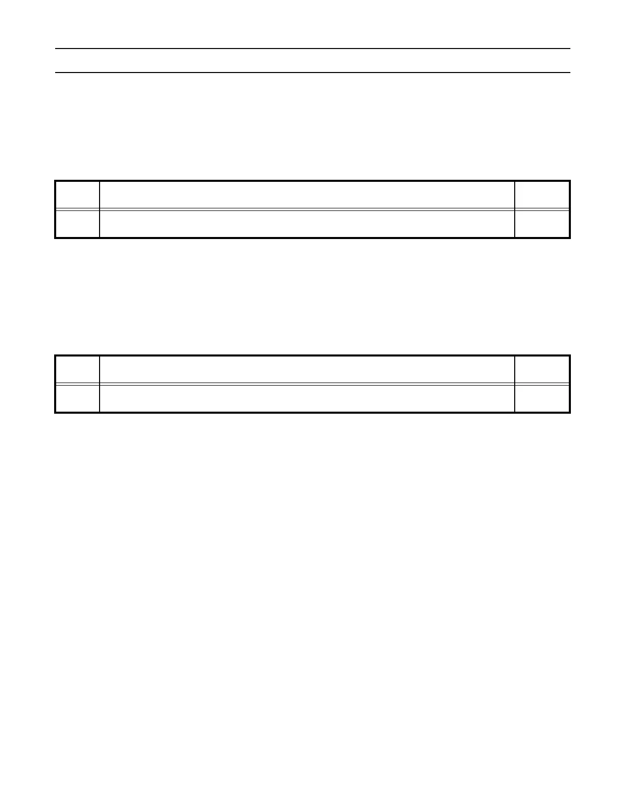
Table 71: GPIO Output Clear Register (IO0CLR - 0xE002800C, IO1CLR - 0xE002801C, IO2CLR - 0xE002802C, IO3CLR -
0xE002803C)
IOCLR Description
Value after
Reset
31:0
Output value CLEAR bits. Bit 0 in IO0CLR corresponds to P0.0 ... Bit 31 in IO0CLR corresponds to
P0.31
0
Table 72: GPIO Direction Register (IO0DIR - 0xE0028008, IO1DIR - 0xE0028018, IO2DIR - 0xE0028028, IO3DIR -
0xE0028038)
IODIR Description
Value after
Reset
31:0
Direction control bits (0 = INPUT, 1 = OUTPUT). Bit 0 in IO0DIR controls P0.0 ... Bit 31 in IO0DIR
controls P0.31
0