SPI Interface 179 May 03, 2004
Philips Semiconductors Preliminary User Manual
LPC2119/2129/2194/2292/2294ARM-based Microcontroller
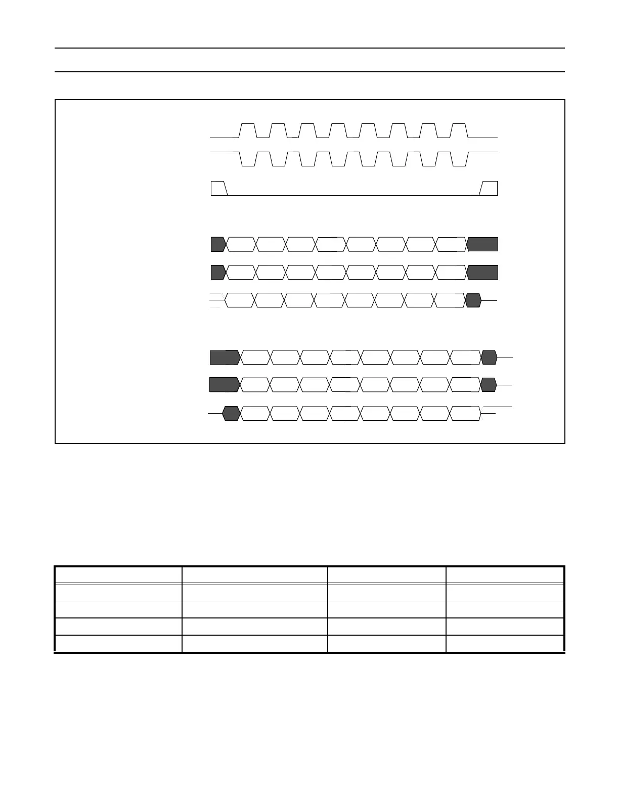
Figure 33: SPI Data Transfer Format (CPHA = 0 and CPHA = 1)
The data and clock phase relationships are summarized in Table 113. This table summarizes the following for each setting of
CPOL and CPHA.
• When the first data bit is driven.
• When all other data bits are driven.
• When data is sampled.
The definition of when an 8 bit transfer starts and stops is dependent on whether a device is a master or a slave, and the setting
of the CPHA variable.
Table 113: SPI Data To Clock Phase Relationship
CPOL And CPHA Settings First Data Driven Other Data Driven Data Sampled
CPOL = 0, CPHA = 0 Prior to first SCK rising edge SCK falling edge SCK rising edge
CPOL = 0, CPHA = 1 First SCK rising edge SCK rising edge SCK falling edge
CPOL = 1, CPHA = 0 Prior to first SCK falling edge SCK rising edge SCK falling edge
CPOL = 1, CPHA = 1 First SCK falling edge SCK falling edge SCK rising edge
Bit 1
12345678
Bit 1 Bit 2 Bit 3 Bit 4 Bit 5 Bit 6 Bit 7 Bit 8
Bit 1 Bit 2 Bit 3 Bit 4 Bit 5 Bit 6 Bit 7 Bit 8
Bit 1 Bit 2 Bit 3 Bit 4 Bit 5 Bit 6 Bit 7 Bit 8
12345678
SCK (CPOL = 0)
SCK (CPOL = 1)
SSEL
CPHA = 0
Cycle # CPHA = 0
MOSI (CPHA = 0)
MISO (CPHA = 0)
CPHA = 1
Cycle # CPHA = 1
MOSI (CPHA = 1)
MISO (CPHA = 1)
Bit 2 Bit 3 Bit 4 Bit 5 Bit 6 Bit 7 Bit 8