176
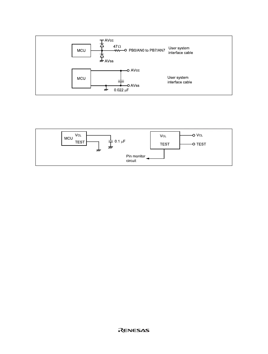
PB0 to PB7 (pins used for AN0 to AN7), AVcc and AVss:
Figure 7.3 User System Interface Circuit for PB0 to PB7, AVcc and AVss Signals
V
CL
and TEST: When V
CL
is connected to GND or the TEST pin is connected to the Vcc level, a warning
message to indicate that the pin connections are incorrect will be displayed when the emulator is connected.
Recheck these pins on the user system.
Figure 7.4 V
CL
and TEST System Interface Circuit

 Loading...


