13. Timer S
puorG92/C61M
page 142
854fo7002,03.raM21.1.veR
2110-1010B90JER
Figures 13.2 to 13.10 show registers associated with the IC/OC base timer, the time measurement func-
tion, and the waveform generating function.
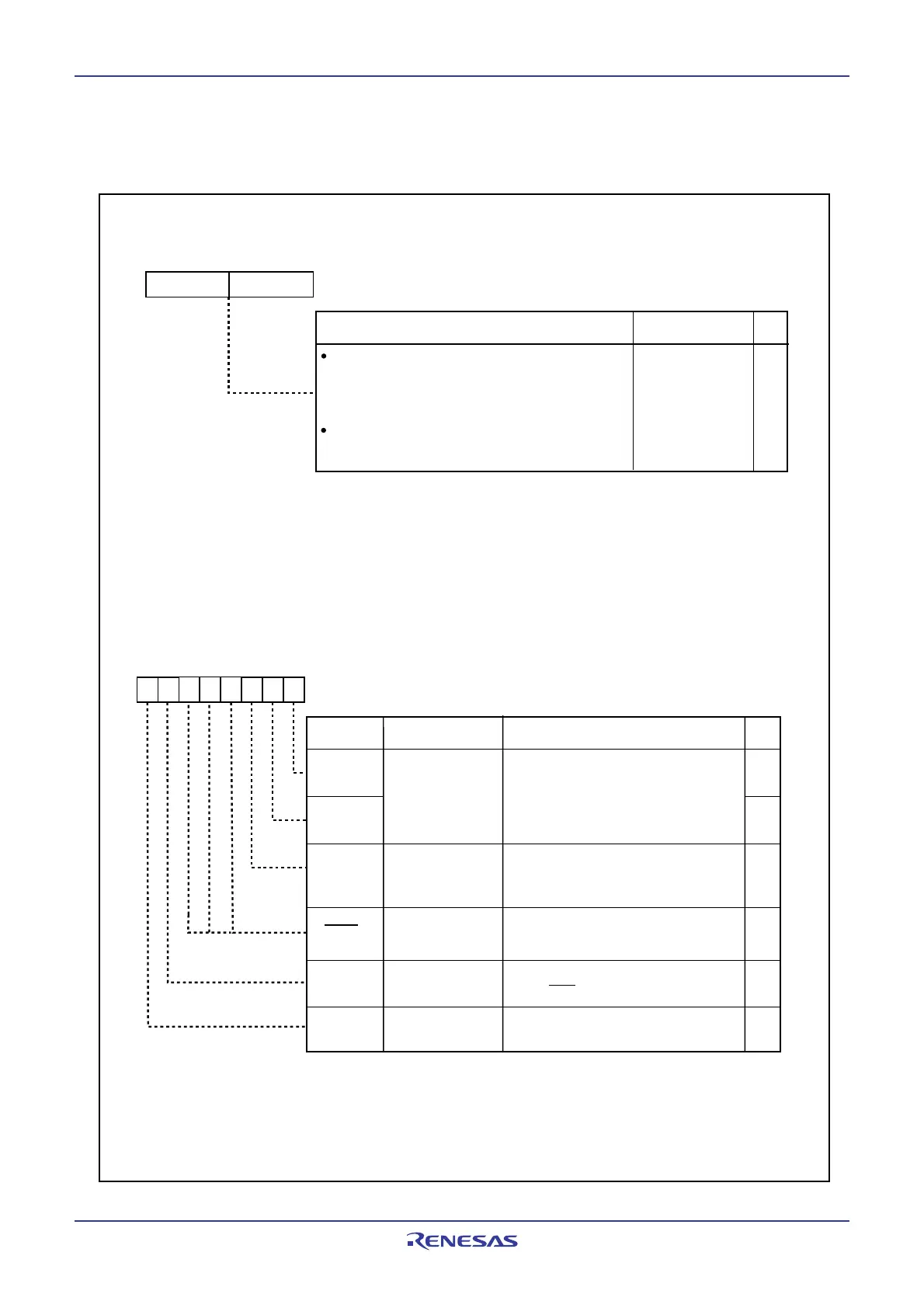
Figure 13.2 G1BT and G1BCR0 Registers
Base Timer Register
(1)
Symbol Address After Reset
G1BT
0321
16
- 0320
16
Undefined
RW
RW
Function
(b7) b0
Setting Range
0000
16
to FFFF
16
b8b15
b7
(b0)
When the base timer is operating:
When read, the value of base timer plus 1 can
be read. When write, the counter starts counting
from the value written. When the base timer is
reset, this register is set to 0000
16.
(2)
When the base timer is reset:
This register is set to 0000
16 but a value read is
undefined. No value is written.
(2)
NOTES:
1.
The G1BT register reflects the value of the base timer, synchronizing with the count source f
BT1
cycles.
2. This base timer stops only when bits BCK1 to BCK0 in the G1BCR0 register are set to 00
2
(count source
clock stop). The base timer operates when bits BCK1 to BCK0 are set to other than 00
2
. When the BTS
bit in the G1BCR1 register is set to 0, the base timer is reset continuously, and remaining set to 0000
16
.
When the BTS bit is set to 1, this state is cleared and the timer starts counting.
Base Timer Control Register 0
Symbol Address After Reset
G1BCR0 032216 0016
RW
RW
RW
RW
RW
RWBit Name FunctionBit Symbol
: Clock stop
: Do not set to this value
: Two-phase input
(1)
: f1 or f2
(2)
b1
0
0
1
1
b0
0
1
0
1
BCK0
BCK1
RST4
Count source
select bit
Channel 7 input
select bit
IT
Base timer
interrupt select bit
0: Bit 15 in the base timer overflows
1: Bit 14 in the base timer overflows
CH7INSEL
0: Do not reset Base timer by matching
G1BTRR
1: Reset Base timer by matching
G1BTRR
(3)
NOTES:
1. This setting can be used when bits UD1 to UD0 in the G1BCR1 register are set to 10
2 (two-
phase signal processing mode). Do not set bits BCK1 and BCK0 to 10
2 in other modes.
2. When the PCLK0 bit in the PCLKR register is set to 0, the count source is f
2 cycles. And when
the PCLK0 bit is set to set to 1, the count source is f
1 cycles.
3. When the RST4 bit is set to 1, set the RST1 bit in the G1BCR1 register to 0.
Base timer reset
cause select bit 4
0: P2
7/OUTC17/INPC17 pin
1: P1
7/INT5/INPC17/IDU pin
Reserved bit Set to 0
(b5-b3)
RW
b7 b6 b5 b4 b3 b2 b1 b0
0
0
0
 Loading...


