14.Serial I/O
puorG92/C61M
page 182
854fo7002,03.raM21.1.veR
2110-1010B90JER
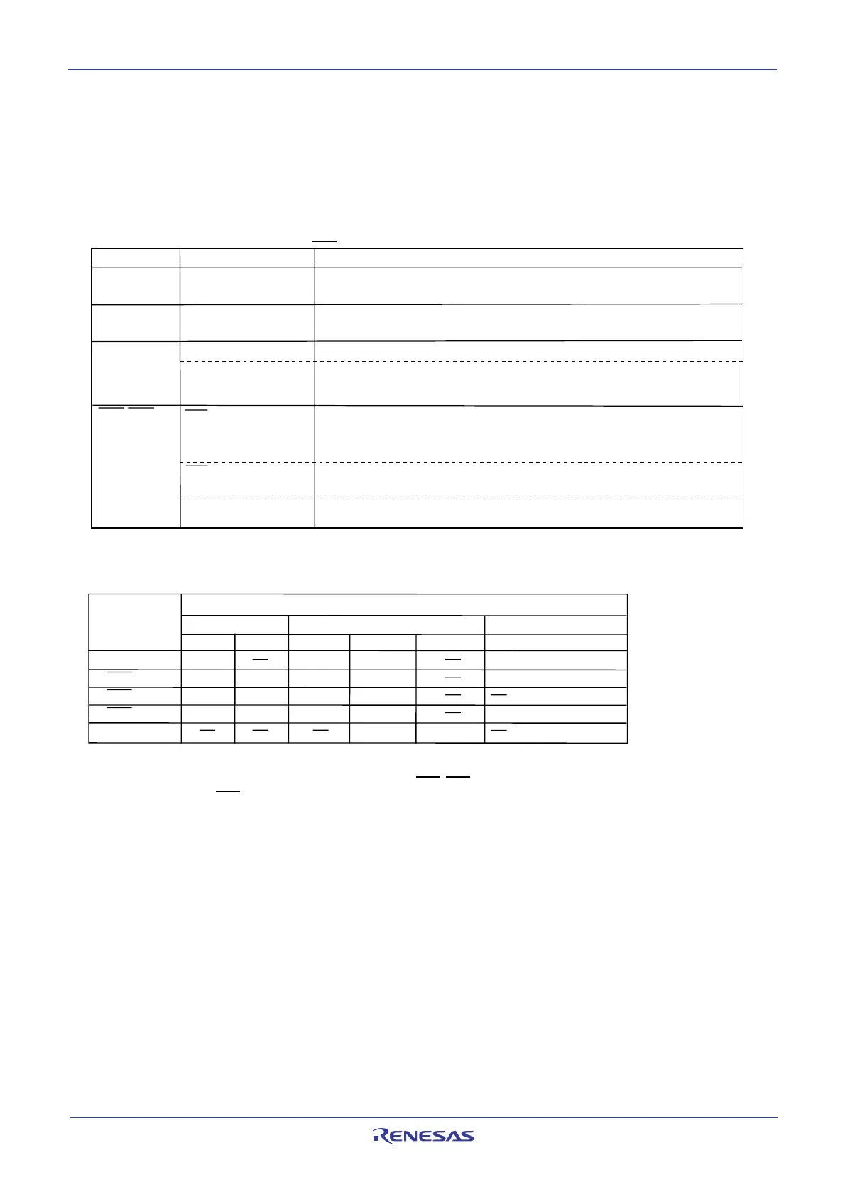
Table 14.3 lists pin functions for the case where the multiple transfer clock output pin select function is
deselected. Table 14.4 lists the P64 pin functions during clock synchronous serial I/O mode.
Note that for a period from when the UARTi operation mode is selected to when transfer starts, the TxDi
pin outputs an “H”. (If the N-channel open-drain output is selected, this pin is in a high-impedance state.)
Table 14.3 Pin Functions (When Not Select Multiple Transfer Clock Output Pin Function)
(1)
Table 14.4 P64 Pin Functions
(1)
Pin Name
Function
Method of Selection
TxDi (i = 0 to 2)
(P6
3
, P6
7
, P7
0
)
Serial data output
Serial data input
Transfer clock output
Transfer clock input
I/O port
(Outputs dummy data when performing reception only)
RxDi
(P6
2
, P6
6
, P7
1
)
CLKi
(P6
1
, P6
5
, P7
2
)
Set the CKDIR bit in the UiMR register to 0
Set the CKDIR bit in the UiMR register to 1
Set the PD6_1 bit and PD6_5 bit in the PD6 register, and the PD7_2 bit in the
PD7 register to 0
Set the PD6_2 bit and PD6_6 bit in the PD6 register, and PD7_1 bit in the PD7
register to 0 (Can be used as an input port when performing transmission only)
Set the CRD bit in the UiC0 register to 0
Set the CRS bit in the UiC0 register to 0
Set the PD6_0 bit and PD6_4 bit in the PD6 register is set to 0, the PD7_3 bit
in the PD7 register to 0
Set the CRD bit in the UiC0 register to 0
Set the CRS bit in the UiC0 register to 1
Set the CRD bit in the UiC0 register to 1
CTS input
RTS output
CTSi/RTSi
(P6
0
, P6
4
, P7
3
)
NOTE:
1: When the U1MAP bit in PACR register is 1 (P7
3
to P7
0
), UART1 pin is assgined to P7
3
to P7
0
.
Pin Function
Bit Set Value
U1C0 register
UCON register
PD6 register
CRD
CRS
RCSP
CLKMD1 CLKMD0
PD6_4
P6
4
1 0 0 Input: 0, Output: 1
CTS1
000 0
RTS
1
10 0
CTS
0
(2
)
0
CLKS
1
0
0
00
1
1
0
1
(3)
NOTES:
1. When the U1MAP bit in PACR register is 1 (P7
3 to P70), this table lists the P70 functions.
2. In addition to this, set the CRD bit in the U0C0 register to 0 (CT0
0/RT00 enabled) and the CRS bit in the
U0C0 register to 1 (RTS
0 selected).
3. When the CLKMD1 bit is set to 1 and the CLKMD0 bit is set to 0, the following logic levels are output:
• High if the CLKPOL bit in the U1C0 register is set to 0
• Low if the CLKPOL bit in the U1C0 register is set to 1
 Loading...


