14. Serial I/O
puorG92/C61M
page 183
854fo7002,03.raM21.1.veR
2110-1010B90JER
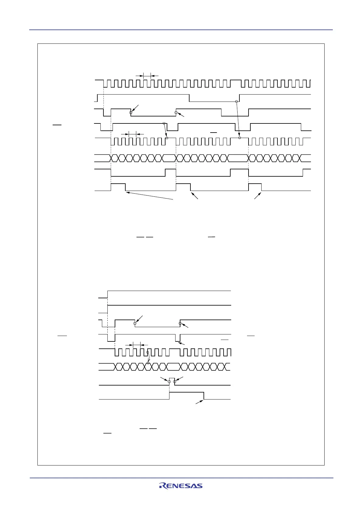
Figure 14.10 Typical transmit/receive timings in clock synchronous serial I/O mode
D0
D1
D2 D3
D4 D5 D6
D7
D0
D1
D2 D3
D4 D5 D6
D7
D0
D1
D2 D3
D4 D5 D6
D7
Tc
T
CLK
Stopped pulsing because the TE bit = 0
Write data to the UiTB register
Tc = T
CLK
= 2(n + 1) / fj
fj: frequency of UiBRG count source (f
1SIO
, f
2SIO
, f
8SIO
, f
32SIO
)
n: value set to UiBRG register
i: 0 to 2
Transfer clock
UiC1 register
TE bit
UiC1 register
TI bit
CLKi
TxDi
“H”
“L”
0
1
0
1
0
1
CTSi
0
1
Stopped pulsing because CTSi = “H
”
1 / fEXT
Write dummy data to UiTB register
UiC1 register
TE bit
UiC1 register
TI bit
CLKi
RxDi
UiC1 register
RI bit
RTSi
“H”
“L”
0
1
0
1
0
1
UiC1 register
RE bit
0
1
Receive data is taken in
Transferred from UiTB register to UARTi transmit register
Read out from UiRB register
f
EXT
: frequency of external clock
Transferred from UARTi receive register
to UiRB registe
r
SiRIC register
IR bit
0
1
D
0
D1
D2 D3
D4 D5 D6
D7
D0
D1
D2
D3 D4
D5
Transferred from UiTB register to UARTi transmit register
Make sure the following conditions are met when input
to the CLKi pin before receiving data is high:
• UiC0 register TE bit is set to 1 (transmit enabled)
• UiC0 register RE bit is set to 1 (Receive enabled)
• Write dummy data to the UiTB register
The above timing diagram applies to the case where the register bits are set as follows:
• The CKDIR bit in the UiMR register is set to 0 (internal clock)
• The CRD bit in the UiC0 register is set to 0 (CTS/RTS enabled); CRS bit is set to 0 (CTS selected)
• The CKPOL bit in the UiC0 register is set to 0 (transmit data output at the falling edge and receive data taken in at the rising edge of the
transfer clock)
• The UiIRS bit is set to 0 (an interrupt request occurs when the transmit buffer becomes empty): U0IRS bit is the bit 0 in the UCON register
U1IRS bit is the bit 1 in the UCON register, and U2IRS bit is the bit 4 in the U2C1 register.
Cleared to 0 when interrupt request is
accepted, or cleared to 0 by program
Cleared to “0” when interrupt request is accepted, or cleared to 0 by program
The above timing diagram applies to the case where the register bits are set
as follows:
• The CKDIR bit in the UiMR register is set to 1 (external clock)
• The CRD bit in the UiC0 register is set to 0 (CTS/RTS enabled);
The CRS bit is set to 1 (RTS selected)
• UiC0 register CKPOL bit is set to 0 (transmit data output at the falling edge and
receive data taken in at the rising edge of the transfer clock)
UiC0 register
TXEPT bit
SiTIC register
IR bit
Even if the reception is completed, the RTS
does not change. The RTS becomes “L”
when the RI bit changes to 0 from 1.
(1) Example of Transmit Timing (Internal clock is selected)
(2) Example of Receive Timing (External clock is selected)
 Loading...


