- 158 -
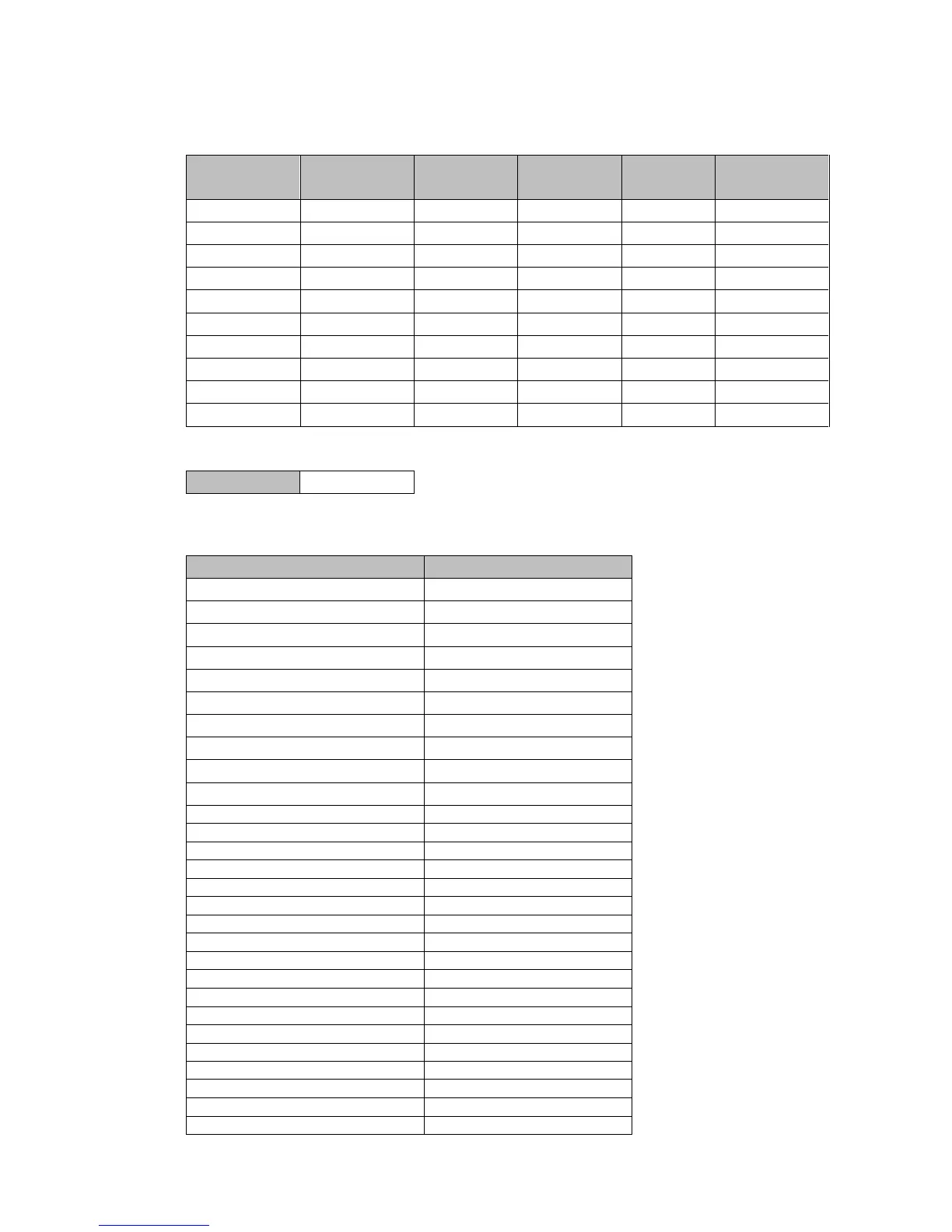
Data Table
Please make a copy of this table for use.
• PID block
PID Block
number
OUT1
P-band
Integral
time
Derivative
time
ARW
OUT2
P-band
1 sec sec %
2 sec sec %
3 sec sec %
4 sec sec %
5 sec sec %
6 sec sec %
7 sec sec %
8 sec sec %
9 sec sec %
10 sec sec %
• Wait value
Wait value
Wait value is common to all steps for each pattern.
• Other setting data (Please use the blank for your own usage.)
Setting item Data
OUT1 proportional cycle sec
OUT2 proportional cycle sec
Number of repetitions times
Pattern link
Communication protocol
Instrument number
Communication speed
bps
Data bit/Parity
Stop bit
Response delay time
ms