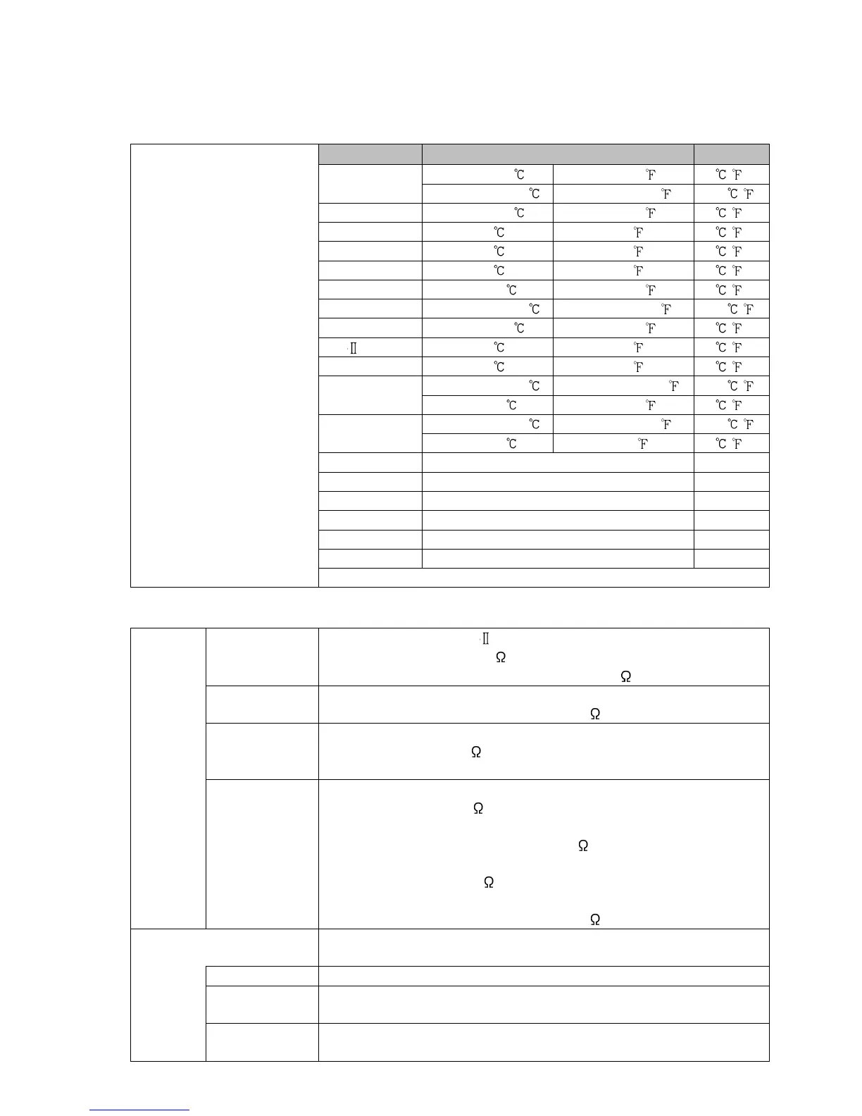
K
-200 to 1370 -328 to 2498 1 ( )
-200.0 to 400.0 -328.0 to 752.0 0.1 ( )
J -200 to 1000 -328 to 1832 1 ( )
R 0 to 1760 32 to 3200 1 ( )
S 0 to 1760 32 to 3200 1 ( )
B 0 to 1820 32 to 3308 1 ( )
E -200 to 800 -328 to 1472 1 ( )
T -200.0 to 400.0 -328.0 to 752.0 0.1 ( )
N -200 to 1300 -328 to 2372 1 ( )
PL-
0 to 1390 32 to 2534 1 ( )
C(W/Re5-26) 0 to 2315 32 to 4199 1 ( )
Pt100
-200.0 to 850.0 -328.0 to 1562.0 0.1 ( )
-200 to 850 -328 to 1562 1 ( )
JPt100
-200.0 to 500.0 -328.0 to 932.0 0.1 ( )
-200 to 500 -328 to 932 1 ( )
4 – 20 mA -2000 to 10000 (*) 1
0 – 20 mA -2000 to 10000 (*) 1
0 – 1 V -2000 to 10000 (*) 1
0 – 5 V -2000 to 10000 (*) 1
1 – 5 V -2000 to 10000 (*) 1
0 – 10 V -2000 to 10000 (*) 1
(*) Scaling and decimal point place selection are possible.
Input
Input
Thermocouple
K, J, R, S, B, E, T, N, PL- , C(W/Re5-26)
External resistance: 100 max.
However, for B input, External resistance: 40 max.
RTD
Pt100, JPt100 3-wire type
Allowable input lead wire resistance: 10 max. per wire
Direct current
0 to 20 mA DC, 4 to 20 mA DC
Input impedance: 50
Allowable input current: 50 mA max.
DC voltage
0 – 1 V DC
Input impedance: 1 M min.
Allowable input voltage: 5 V DC max.
Allowable signal source resistance: 2 k max.
0 – 5 V DC, 1 – 5 V DC, 0 – 10 V DC
Input impedance: 100 k min.
Allowable input voltage: 15 V DC max.
Allowable signal source resistance: 100 max.
Event input
(C5W,EIW,EIT, C5,EIoptions)
Input point 2 points
Circuit current
when closed
Approx. 16 mA
Action Edge action
When the power is turned ON, level action is engaged.