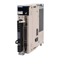
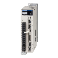
6.1 I/O Signal Allocations
6.1.2 Output Signal Allocations
6-7
6.1.2
Output Signal Allocations
You can allocate the desired output signals to pins 25 to 30 and 37 to 39 on the I/O signal con-
nector (CN1). You set the allocations in the following parameters: Pn50E, Pn50F, Pn510,
Pn512, Pn513, Pn514, and Pn517.
Output signals are allocated as shown in the following table.
Refer to Interpreting the Output Signal Allocation Tables and change the allocations accord-
ingly.
Interpreting the Output Signal Allocation Tables
• The signals that are not detected are considered to be OFF. For example, the /COIN (Position-
ing Completion) signal is considered to be OFF during speed control.
• Reversing the polarity of the /BK (Brake) signal, i.e., changing it to positive logic, will prevent
the holding brake from operating if its signal line is disconnected. If you must change the polar-
ity of this signal, verify operation and make sure that no safety problems will exist.
• If you allocate more than one signal to the same output circuit, a logical OR of the signals will
be output.
25 and 26 27 and 28 29 and 30 37 38 39
123 4056/COIN
Disabled
(Not Used)
CN1 Pin No.
Output
Signal
Positioning
Completion
Pn50E = n.X
Output Signal Name
and Parameter
: Default settings.
These columns give the parameter settings to use. Signals
are allocated to CN1 pins according to the settings.