2-36 Mechanism Configuration and Operating Principles Rev. A
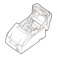
Operation panel and cover open sensor circuits
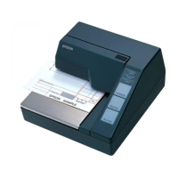
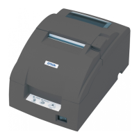
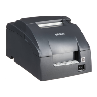
There are five LEDs on the operation panel (POWER, ERROR, RECEIPT OUT, JOURNAL OUT,
and SLIP) and two buttons (RECEIPT FEED, and JOURNAL/SLIP FEED). The cover open
sensor uses a photosensor.
These parts are mounted directly on the switch PCB unit, which is linked to the main PCB
assembly via connectors (CN8).
55 AB 2 A 2 I TTL Address signal Bit 2
56 AB 3 A 3 I TTL Address signal Bit 3
57 AB 4 A 4 I TTL Address signal Bit 4
58 (R/W
)(R/W) I TTL Read/write signal
59 (CS
)(CS) I TTL Chip select signal L = select
60 (E
)(E)ITTLEnable signal
61 ASTB ASTB I TTL Address latch enable signal
62 ALB 0 A 16 O TTL Address signal Bit 16
63 ABL 1 A 17 O TTL Address signal Bit 17
64 ABL 2 A 18 O TTL Address signal Bit 18
65 ABL 3 A 19 O TTL Address signal Bit 19
66 ABL 4 N. C O TTL Unused (open)
67 ABL 5 N. C O TTL Unused (open)
68 ABL 6 N. C O TTL Unused (open)
69 ABL 7 N. C O TTL Unused (open)
70 GND — — GND Power supply
71 GND — — GND Power supply
72 (V
ss
) — — +5V Power supply
73 DB 0 D 0 I/O TTL Data signal Bit 0
74 DB 1 D 1 I/O TTL Data signal Bit 1
75 DB 2 D 2 I/O TTL Data signal Bit 2
76 DB 3 D 3 I/O TTL Data signal Bit 3
77 DB 4 D 4 I/O TTL Data signal Bit 4
78 DB 5 D 5 I/O TTL Data signal Bit 5
79 DB 6 D 6 I/O TTL Data signal Bit 6
80 DB 7 D 7 I/O TTL Data signal Bit 7
Table 2-2. Gate Array Pin Assignments (continued)
Pin number Gate array function Signal designation` I/O Level Description
CONFIDENTIAL
 Loading...