4-51
BUS OPERATION
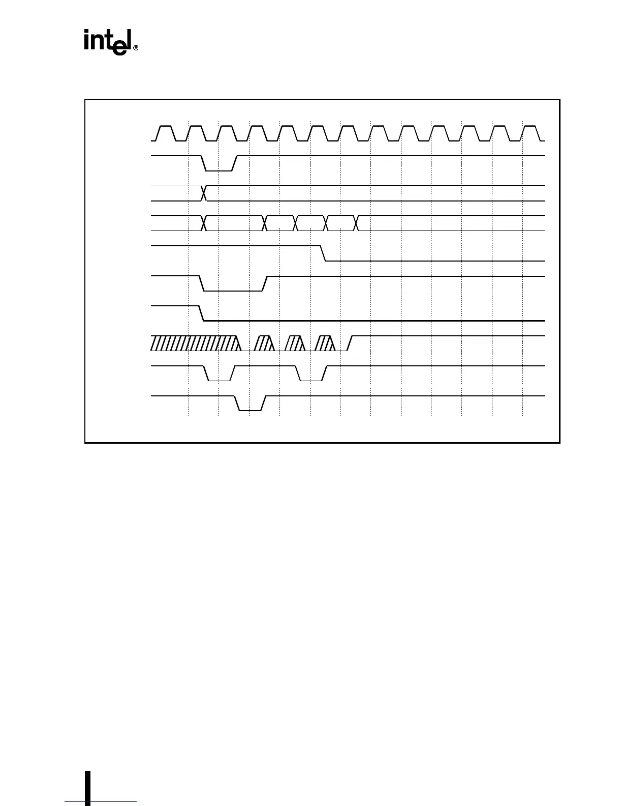
Figure 4-37. Basic Burst Read Cycle
4.4.2.1 Non-Cacheable Burst Operation
When CACHE# is asserted on a read cycle, the processor follows with BLAST# high when
KEN# is asserted. However, the converse is not true. The Write-Back Enhanced IntelDX4 pro-
cessor may elect to read burst data that are identified as non-cacheable by either CACHE# or
KEN#. In this case, BLAST# is also high in the same cycle as the first BRDY# (in clock four).
To improve performance, the memory controller should try to complete the cycle as a burst cycle.
The assertion of CACHE# on a write cycle signifies a replacement or snoop write-back cycle.
These cycles consist of four doubleword transfers (either bursts or non-burst). The signals KEN#
and WB/WT# are not sampled during write-back cycles because the processor does not attempt
to redefine the cacheability of the line.
4.4.2.2 Burst Cycle Signal Protocol
The signals from ADS# through BLAST#, which are shown in Figure 4-37, have the same func-
tion and timing in both Standard Bus and Enhanced Bus modes. Burst cycles can be up to 16-
bytes long (four aligned doublewords) and can start with any one of the four doublewords. The
sequence of the addresses is determined by the first address and the sequence follows the order
242202-149
CLK
ADS#
A31–A4
M/IO#
D/C#
W/R#
A3–A2
BLAST#
CACHE#
BRDY#
WB/WT#
12345678910111213
PCD
KEN#
0 4 8 C