7-31
PERIPHERAL SUBSYSTEM
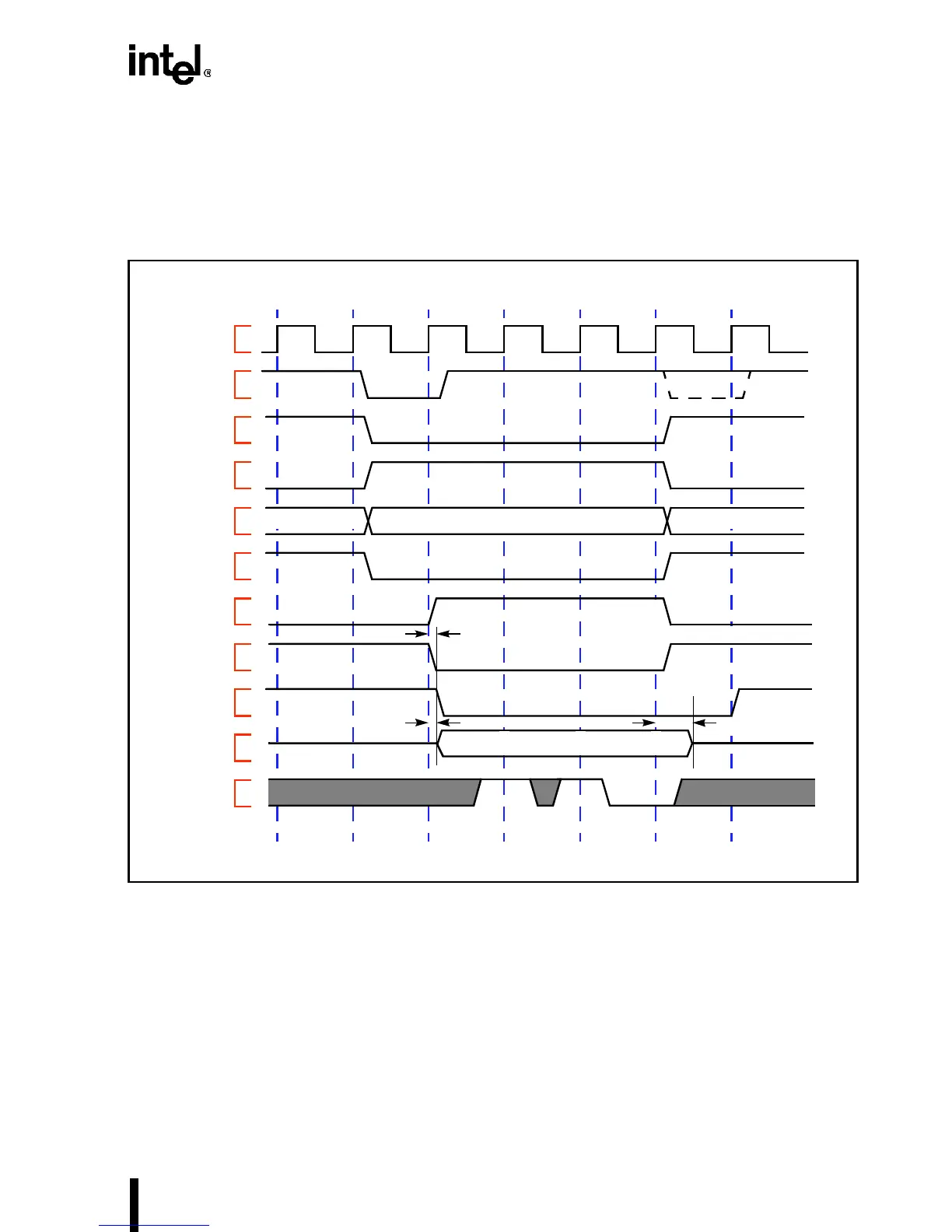
7.3.2 Write Cycle Timings
The I/O write cycle is similar to the I/O read cycle with the exception of W/R# being asserted
high when sampled rather than low from the Intel486 processor side. This is shown in Figures
7-15 and 7-16.
Figure 7-15. I/O Write Cycle Timings
The timing of the remaining signals (the address and status signals) is similar to that of I/O read
cycle timings. The processor outputs data in T2. The I/O write signal (IOW#) may be asserted
one or two clocks after the chip select. The exact delay between the chip select and the IOW#
varies according to the write requirements of the I/O device. Data is written into the I/O device
on the rising edge of IOW#, and the processor stops driving data once RDY# data is sampled ac-
tive. The critical timings for the I/O write cycle are shown in Figure 7-16.
CLK
ADS#
M/IO#
D/C#
A31–A2
W/R#
IOCYC
IOW#
CS#
DATA
RDY#
From CPU
TW
VD
T2 T2 T2 T2T1 T1
TD
VD TD
FD