EMBEDDED Intel486™ PROCESSOR HARDWARE REFERENCE MANUAL
7-32
Figure 7-16. I/O Write Cycle Timing Analysis
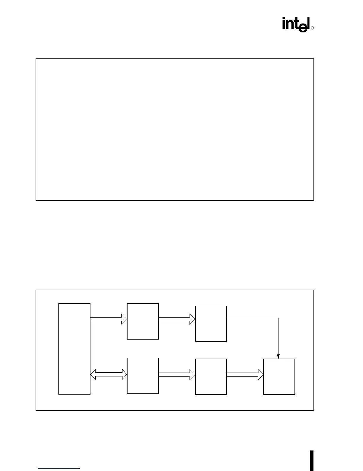
Latches and data buffers can improve processor write performance. In Figure 7-17, I/O addresses
and data are both latched in a configuration called a posted write. Posted writes help increase sys-
tem performance by allowing the processor to complete a cycle without wait states. Once the data
and address are latched, RDY# can be asserted during the first T2 of an I/O write cycle. Thus, the
processor operation and the write cycle to the peripheral device can continue simultaneously.
This is illustrated in Figure 7-18. The write cycle appears to be only two clocks long (from ADS#
to RDY#) because the actual write overlaps other CPU bus cycles.
Figure 7-17. Posted Write Circuit
TW
VD
Write Signal Valid Delay
TW
VD
= T
PLDpd
= 10 ns
TD
VD
Write Data Valid Delay
TD
VD
= T
VD
†
+ T
BUFpd
= 19 + 9 = 28 ns
TD
FD
Write Data Float Time
TD
FD
= T
FD
†
– T
BUFpd
= 0 + 9 = 9 ns
†
T
VD
= T
10
= Intel486™ processor write data valid delay (33 MHz)
T
FD
= T
11
= Intel486 processor write data float delay (33 MHz)
I/O
Device
I/O
Data
Latch
I/O
Address
Decode
I/O
Address
Latch
Data
Buffer
Address
Intel486™
Processor
Data
I/O Write
Data Bus