7-21
PERIPHERAL SUBSYSTEM
7.2.2 Bus Control Signal Description
The following list describes the input/output signals for the bus control logic.
7.2.2.1 Processor Interface
ADS#—Address Status. This input signal to the bus controller is connected directly to the pro-
cessor’s ADS# output. It indicates that a valid bus cycle definition and address are available on
the cycle definition lines and address bus. ADS# is driven active at the same time when addresses
are driven.
M/IO#—Memory/Input-Output Signal
D/C#—Data/Control
W/R#—Write/Read (Input signals to bus controller)
These signals are connected directly to the Intel486 processor’s bus cycle status outputs. For the
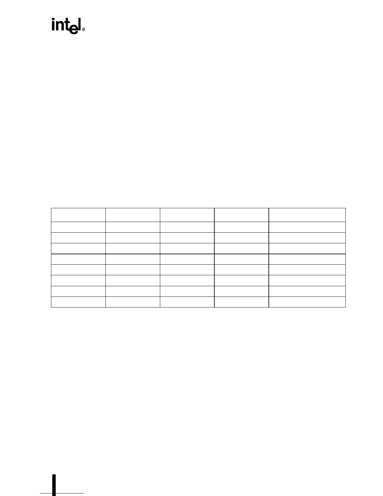
Intel486 processor, they are valid when ADS# is asserted. Table 7-11 describes the bus cycles of
various combinations of M/IO#, D/C# and W/R# signals.
RDY#—Ready Output Signal. This signal is connected directly to the Intel486 processor’s
RDY# input and indicates that the current bus cycle is complete. It also indicates that the I/O de-
vice has returned valid data to the Intel486 processor’s data pins following an I/O write cycle. For
the Intel486 processor, RDY# is ignored when the bus is idle and at the end of the first clock of
the bus cycle. The signal is utilized in wait state generation which is covered in the next section.
CLK#—Clock Input Signal. This signal provides the fundamental timings for the bus control
logic and is synchronous with the processor’s clock. All of the external timings are specified with
respect to the rising edge of the clock.
IOCYC—I/O Interface Signals. The IO cycle output signal is generated at the rising clock edge
following ADS#, M/IO#, D/C and W/R# being active. The signal indicates that an I/O cycle is
taking place and is used to enable the address decoder.
Table 7-11. Bus Cycle Definitions
M/IO# D/C# W/R# ADS# Bus Cycle Initiated
0 0 0 0 Interrupt acknowledge
0 0 1 0 Halt/special cycle
0100 I/O read
0110 I/O write
1000Code read
1010Reserved
†
1100Memory read
1110Memory write
NOTE:
†
Intel reserved. Do not use.