EasyManua.ls Logo

Intel Embedded Intel486 User Manual

Intel Embedded Intel486
334 pages
To Next Page IconTo Next Page
To Previous Page IconTo Previous Page
Page #145 background image
5-5
MEMORY SUBSYSTEM DESIGN
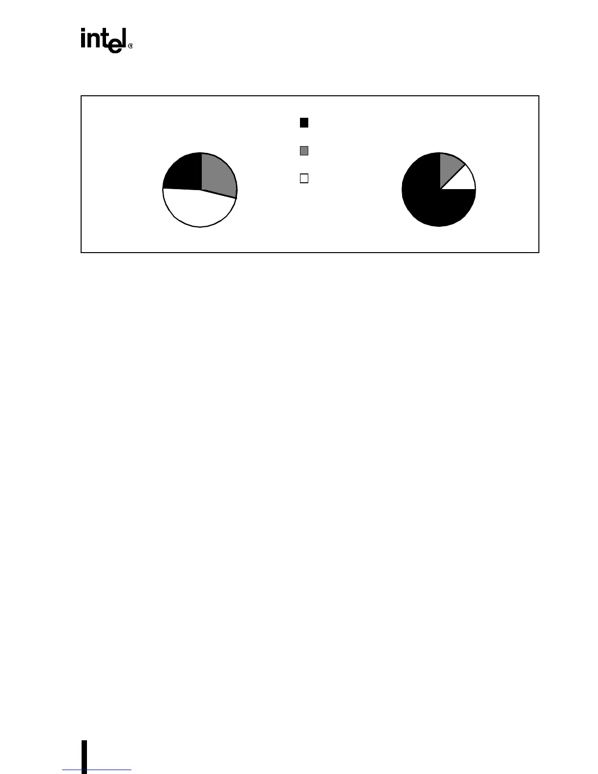
Figure 5-3. Intel386 Processor Bus Cycle Mix/Intel486™ Processor Bus Cycle Mix
It seems obvious that many of these write cycles would be consecutive. In fact, 70% of all write
cycles are consecutive. Furthermore, 50% of all write cycles occur three in-a-row. It is obvious
from these statistics that optimizing the memory subsystem for write cycles can improve perfor-
mance. But it is important to optimize the memory system for consecutive write cycles. Improv-
ing individual write cycle latency does not buy much performance improvement if subsequent
write cycles suffer.
5.2.4 Improving Write Cycle Latency
5.2.4.1 Interleaving
The interleaving technique is used to support the burst bus feature of the Intel486 processor. The
use of this technique allows the DRAM to supply a dword every clock during burst cycles. Inter-
leaving proves to be very useful in Intel486 processor memory designs. Without its use, DRAM
timings such as T
PC
(Page Mode Cycle time) and T
CP
(CAS Precharge time) would prevent zero
wait state access at 33 MHz.
5.2.4.2 Write Posting
Analysis has shown that, in general, 6% degradation in performance can be expected for every
additional wait state added to write cycles. This analysis was performed by measuring the CPU
clocks required to execute several applications.
A technique called write posting can be used to improve write cycle latency. Write posting uses
data registers that hold write data during write cycles. This technique allows consecutive write
cycles to be overlapped. It also allows write cycles to be overlapped with L2 cache cycles and
reduces overall write miss latency.
Using the write posting technique adds complexity to the system logic. It is important to deter-
mine the performance improvement realized by using this technique. This question is especially
pertinent when we consider the logic already implemented in the Intel486 processor to improve
write performance. The internal Intel486 write buffers decouple the processor execution unit
from the external bus.
21.65%
35.90%
42.45%
74.84%
12.79%
12.37
Write
Prefetch
Read
Intel386™ Bus Cycle Mix Intel486™ Bus Cycle Mix

Table of Contents

Question and Answer IconNeed help?

Do you have a question about the Intel Embedded Intel486 and is the answer not in the manual?

Intel Embedded Intel486 Specifications

General IconGeneral
BrandIntel
ModelEmbedded Intel486
CategoryComputer Hardware
LanguageEnglish

Summary

Introduction

Processor Features

Details core features like 32-bit RISC core, pipelining, on-chip cache, and MMU.

On-chip Cache

Details the 8/16-Kbyte unified cache, its protocols, and line fills.

Internal Architecture

Instruction Pipelining

Explains how instructions are processed in stages for improved performance.

Cache Unit

Covers cache operation, including hits, misses, line fills, and update policies.

Bus Operation

Data Transfer Mechanism

Explains how data operands of various lengths are transferred over the bus.

Locked Cycles

Covers atomic memory access using the LOCK# pin for read-modify-write operations.

Memory Subsystem Design

Improving Write Cycle Latency

Covers techniques like interleaving and write posting to reduce write latency.

Second-Level Cache

Explains the advantages and performance benefits of using an L2 cache.

Peripheral Subsystem

System Bus Design

PCI BUS: SYSTEM DESIGN EXAMPLE

Introduces the PCI bus, its features, and its implementation in embedded systems.

Performance Considerations

Instruction Execution Performance

Reviews how Intel486 processors achieve faster instruction execution and compares with earlier processors.

Internal Cache Performance Issues

Analyzes the on-chip cache's organization, size, and impact on performance.

On-Chip Write Buffers

Details the function of write buffers in reducing latency and enhancing write performance.

Second-Level Cache Performance Considerations

Explains the advantages and performance benefits of using an L2 cache.

Floating-Point Performance

Analyzes the floating-point unit's performance, execution sequences, and on-chip interface.

Physical Design and System Debugging

Power Dissipation and Distribution

Discusses power dissipation, capacitive loading, and power/ground planes.

High-Frequency Design Considerations

Covers management of transmission lines, impedance control, and EMI.

Latch-Up

Covers prevention of latch-up by observing voltage limits and using proper layout.

Clock Considerations

Discusses requirements for clock signals, skew, and loading effects.

Thermal Characteristics

Explains thermal specifications, junction temperature calculation, and heatsink usage.

Building and Debugging the Intel486™ Processor-Based System

Outlines steps for building and debugging the system incrementally.

Related product manuals